

Semiconductor device and manufacturing method thereof
a semiconductor and semiconductor technology, applied in the direction of transistors, vacuum evaporation coatings, coatings, etc., can solve the problems of significant signal delay due to wiring resistance, hinder the rapid operation of thin film transistors, etc., and achieve low parasitic capacitance, low parasitic capacitance, and low cost
- Summary
- Abstract
- Description
- Claims
- Application Information
AI Technical Summary
Benefits of technology
Problems solved by technology
Method used
Image

Examples
embodiment 1
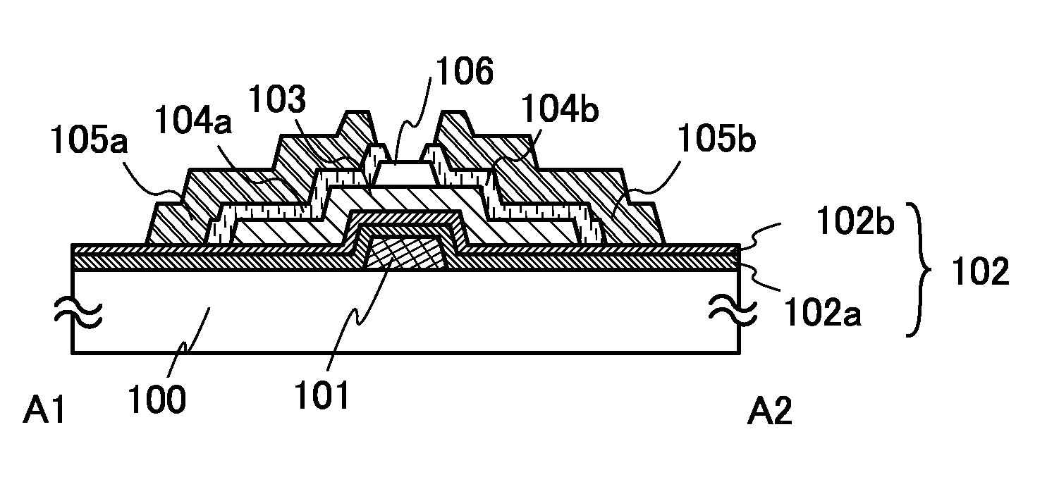
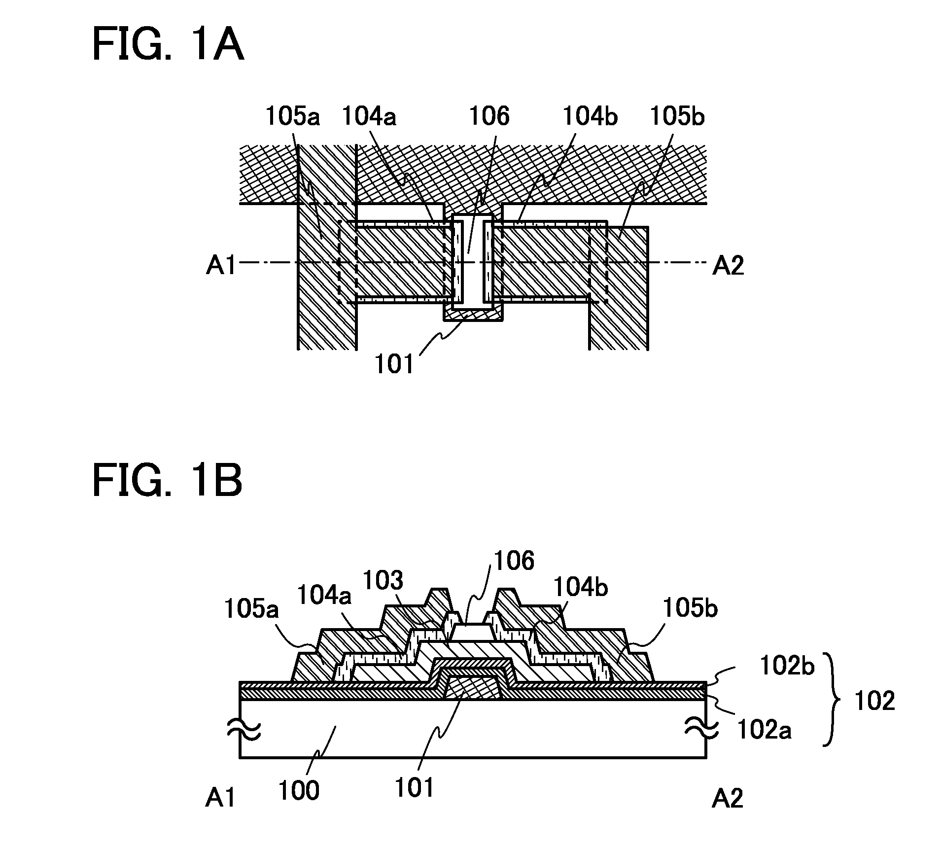
[0083]In this embodiment, a thin film transistor and a manufacturing process thereof will be described with reference to FIGS. 1A and 1B and FIGS. 2A to 2D.
[0084]FIGS. 1A and 1B illustrate a thin film transistor having a bottom gate structure according to this embodiment. FIG. 1A is a plan view and FIG. 1B is a cross-sectional view taken along line A1-A2 in FIG. 1A. In the thin film transistor illustrated in FIGS. 1A and 1B, a gate electrode 101 is formed over a substrate 100; a gate insulating film 102 is formed over the gate electrode 101; an amorphous oxide semiconductor layer 103 functioning as a channel formation region is formed over the gate electrode 101 with the gate insulating film 102 interposed therebetween; a channel protective layer 106 is formed in a region overlapping with the channel formation region of the amorphous oxide semiconductor layer 103; buffer layers 104a and 104b are formed over the amorphous oxide semiconductor layer 103; and source and drain electrode ...
embodiment 2
[0145]In this embodiment, the structure of a thin film transistor in which a buffer layer contains formed using an oxide semiconductor having n-type conductivity and containing In, Ga, and Zn, which is different from the structure of Embodiment 1, will be described with reference to FIGS. 3A1 to 3D. In addition, in this embodiment, the same reference numerals are used for the same portions as those in Embodiment 1 and detailed description of the portions is omitted.
[0146]Through a similar process to that of Embodiment 1, a channel protective layer 106 is formed using an insulating film in a region that overlaps a channel formation region of a semiconductor layer 103 as illustrated in FIG. 3A1. Note that by the etching processing of the channel protective layer 106, the surface of the semiconductor layer 103 to which buffer layer 104 are to be bonded may be etched as illustrated in FIG. 3A2. By etching the surface of the oxide semiconductor layer to which the buffer layer 104 are to ...
embodiment 3
[0157]In this embodiment, the structure of a thin film transistor including a buffer layer, which is different from the structures of Embodiments 1 and 2, will be described with reference to FIGS. 4A to 4D. In addition, in this embodiment, the same reference numerals are used for portions the same as those in Embodiment 1 and a detailed description of the portions is omitted.
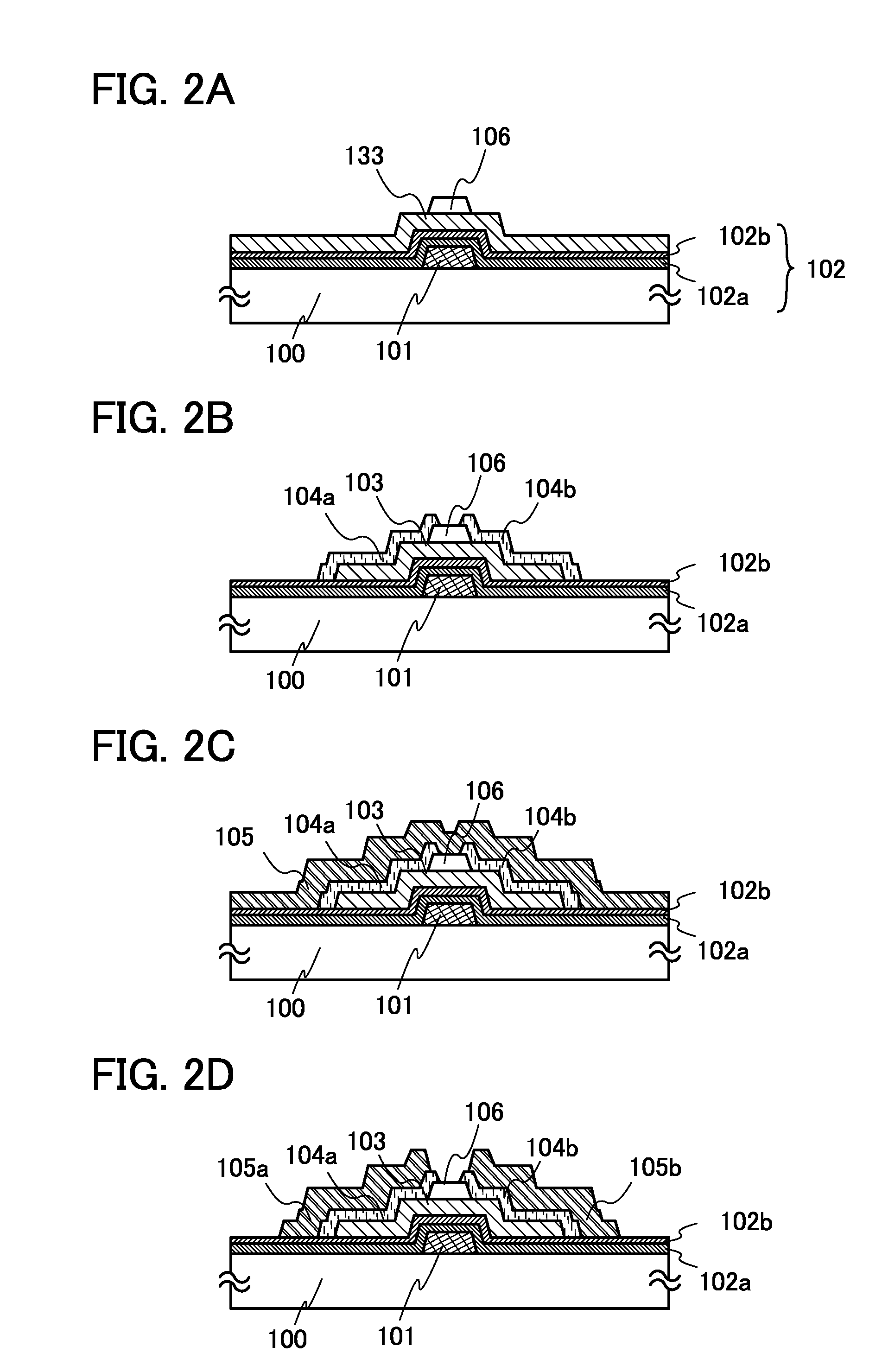
[0158]Through a process similar to that of Embodiment 2, a channel protective layer 106 is formed over a semiconductor film 133 of oxide containing In, Ga, and Zn (IGZO) to be a semiconductor layer 103 as illustrated in FIG. 4A.
[0159]In this embodiment, without formation of the semiconductor layer 103 by selective etching of the semiconductor film 133, an oxide semiconductor film having n-type conductivity and containing In, Ga, and Zn to be buffer layers 104a and 104b is formed over the semiconductor film 133 by a method similar to that of Embodiment 2. Next, the buffer layers 104a and 104b and the semiconducto...
PUM
| Property | Measurement | Unit |
|---|---|---|
| Electrical conductivity | aaaaa | aaaaa |
| Semiconductor properties | aaaaa | aaaaa |
| Carrier concentration | aaaaa | aaaaa |
Abstract
Description
Claims
Application Information