

Method for producing semiconductor device
- Summary
- Abstract
- Description
- Claims
- Application Information
AI Technical Summary
Benefits of technology
Problems solved by technology
Method used
Image

Examples
embodiment 1
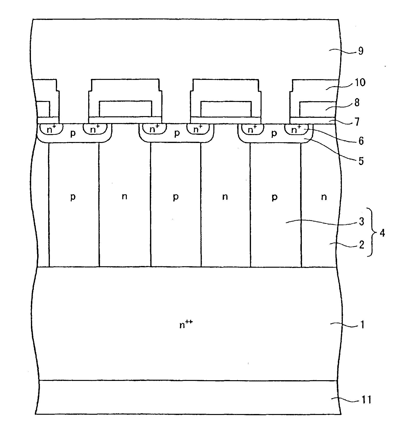
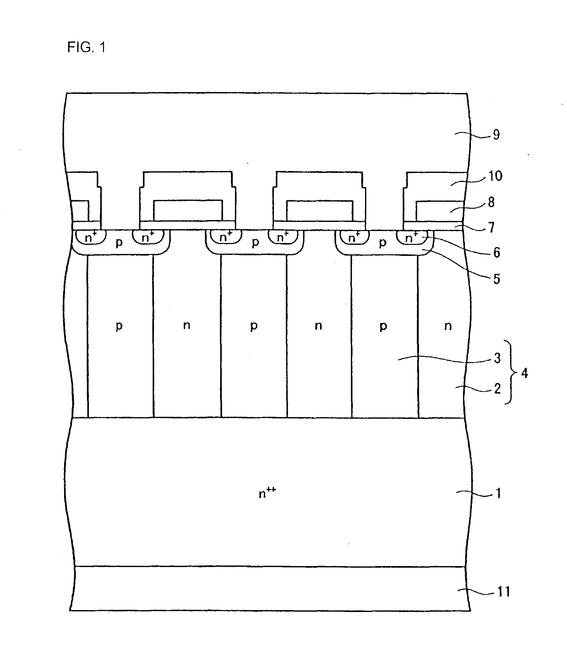
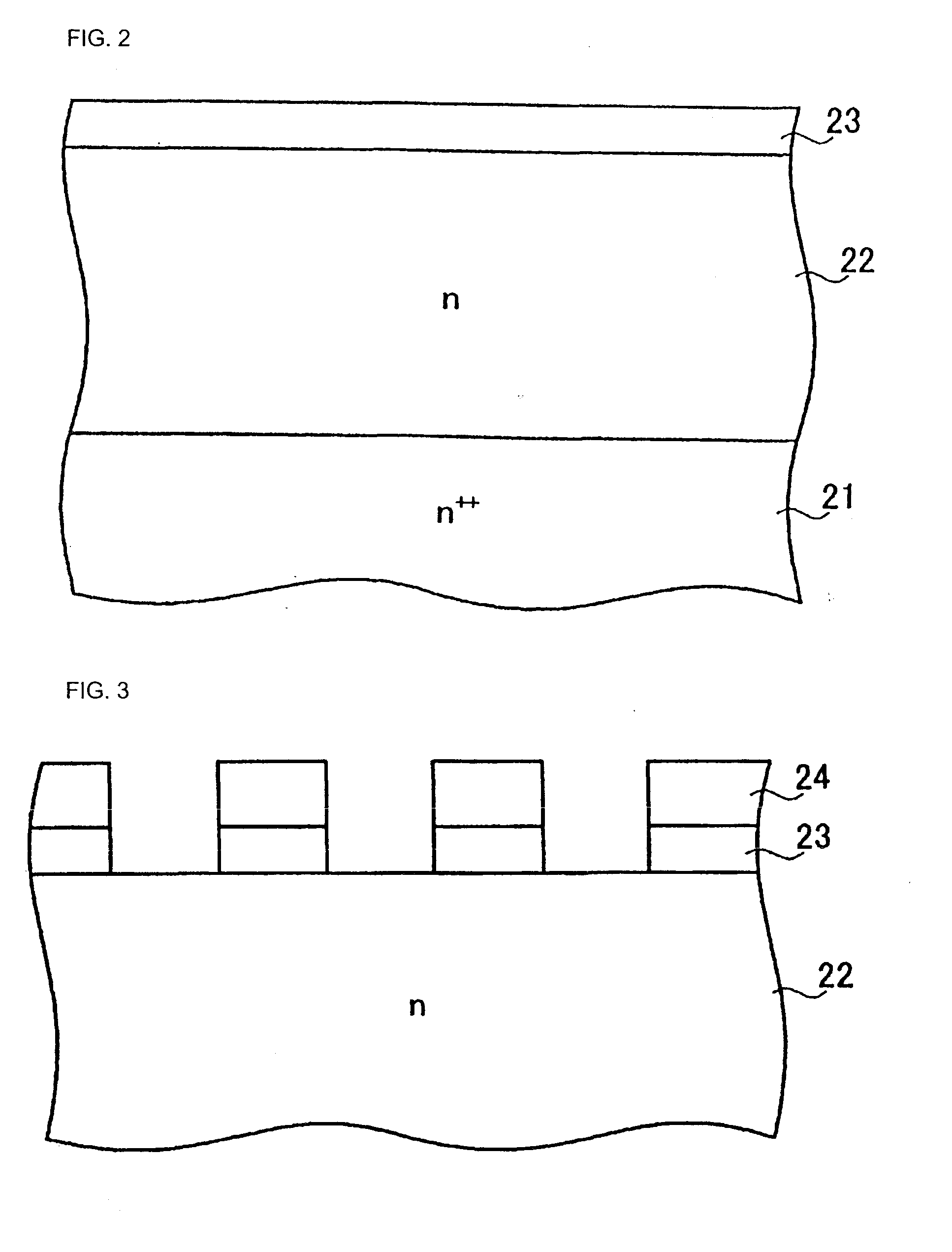
[0053]FIGS. 2 to 11 are sectional views showing a semiconductor device produced by a production method according to First, an n-type low-resistance silicon substrate (n++ substrate) 21 is prepared, and an n-type semiconductor 22 is epitaxially grown on the surface of the substrate. The n-type low-resistance silicon substrate 21 serves as the n++ drain layer 1. Next, a mask oxide film 23 is formed on the surface of the n-type semiconductor 22 by a thermal oxidation method, such as a pyrogenic oxidation method (FIG. 2). Then, a mask nitride film 24 is formed on the surface of the mask oxide film 23. Next, a resist film (not shown) is applied to the surface of the mask nitride film 24. Then, the mask oxide film 23 and the mask nitride film 24 (hereafter referred to as a mask laminated film) are opened at portions above trench forming regions by photolithography and etching. Then, the resist film is removed (FIG. 3).
[0054]Next, for example, the semiconductor device being in the state s...
embodiment 3
[0072]In Embodiment 3, the initial thickness of the mask oxide film 29 is 2.4 μm, for example. In addition, the thickness of the remaining portion of the mask oxide film 29 is 2.0 μm, for example, after the etching process for forming the trenches. Furthermore, by the etching for the mask oxide film 29 performed after the trenches 25 are embedded with the p-type semiconductor 27, the mask oxide film 29 is thinned to 0.8 μm, for example.
[0073]Even when the trenches are completely embedded with the p-type semiconductor 27, the thickness of the mask oxide film 29 is sufficiently large to the extent that the p-type semiconductor 27 is not grown on the surface of the mask oxide film 29. In addition, the effect of the second exposed portions of the n-type semiconductor 22 is similar to that of Embodiment 1.
[0074]As described above, Embodiment 3 can obtain effects similar to those of Embodiment 1.
PUM
 Abstract
Description
Claims
Application Information