Sic single crystals with reduced dislocation density grown by step-wise periodic perturbation technique

a technology of periodic perturbation and single crystals, which is applied in the direction of single crystal growth, polycrystalline material growth, chemistry apparatus and processes, etc., can solve the problems of difficult to clearly separate different types of dislocations through molten koh etching methods on these kinds of samples, and the shape of etch pits in heavily nitrogen-doped n+sic substrates is usually not well defined, so as to improve the purity of growth components, reduce the generation of dislocation

Inactive Publication Date: 2010-02-11
II VI
View PDF7 Cites 34 Cited by
  • Summary
  • Abstract
  • Description
  • Claims
  • Application Information

AI Technical Summary

Benefits of technology

[0018]Conventional and well-established measures can be applied to the PVT sublimation growth process in order to eliminate or reduce the generation of dislocations during growth. These measures include better purity of the growth components; degassing and vacuum baking of the graphite furniture and source at elevated temperatures; and moderation of the temperature gradients.
[0019]The reference “Basal Plane Dislocation Dynamics in Highly p-Type Doped Versus Highly n-Type Doped SiC”, by P. J. Wellmann et al., International Conference on Silicon Carbide and Related Materials, 2005, Pittsburgh, reports the study of the incorporation of an n-type layer during the growth of aluminum doped p-type SiC, using over-compensation by nitrogen, and followed the fraction of BPD in total dislocations through the crystal. The focus of the study was on the comparison between p-type and n-type

Problems solved by technology

Moreover, the shape of etch pits in heavily nitrogen-doped n+SiC substrates are usually not well defined.
Moreover, these etch pits tend to be slightly asymmetric.
As a result, it is difficult to clearly separate different types of dislocations through molten KOH etching methods on these kinds of samples.
However, this difficulty does not affect the measurement of total dislocation density.
Consequently, most of the threading defects and a fraction of BPDs penetrate from the substrate into the epilayer.
In addition, new defects can emerge at the substrate-epitaxial layer interface as a result of interaction between various types of dislocations and the step flow.
As is well-known to those skilled in the art of SiC growth and epitaxy, micropipes and d

Method used


Image

  • Sic single crystals with reduced dislocation density grown by step-wise periodic perturbation technique
  • Sic single crystals with reduced dislocation density grown by step-wise periodic perturbation technique
  • Sic single crystals with reduced dislocation density grown by step-wise periodic perturbation technique

Examples


Embodiment Construction

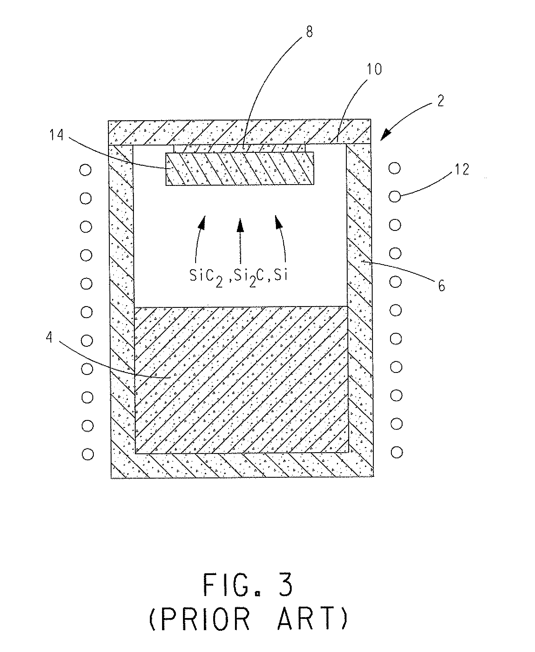
[0040]The following detailed description will be made with reference to the accompanying figures where like reference numbers correspond to like elements.

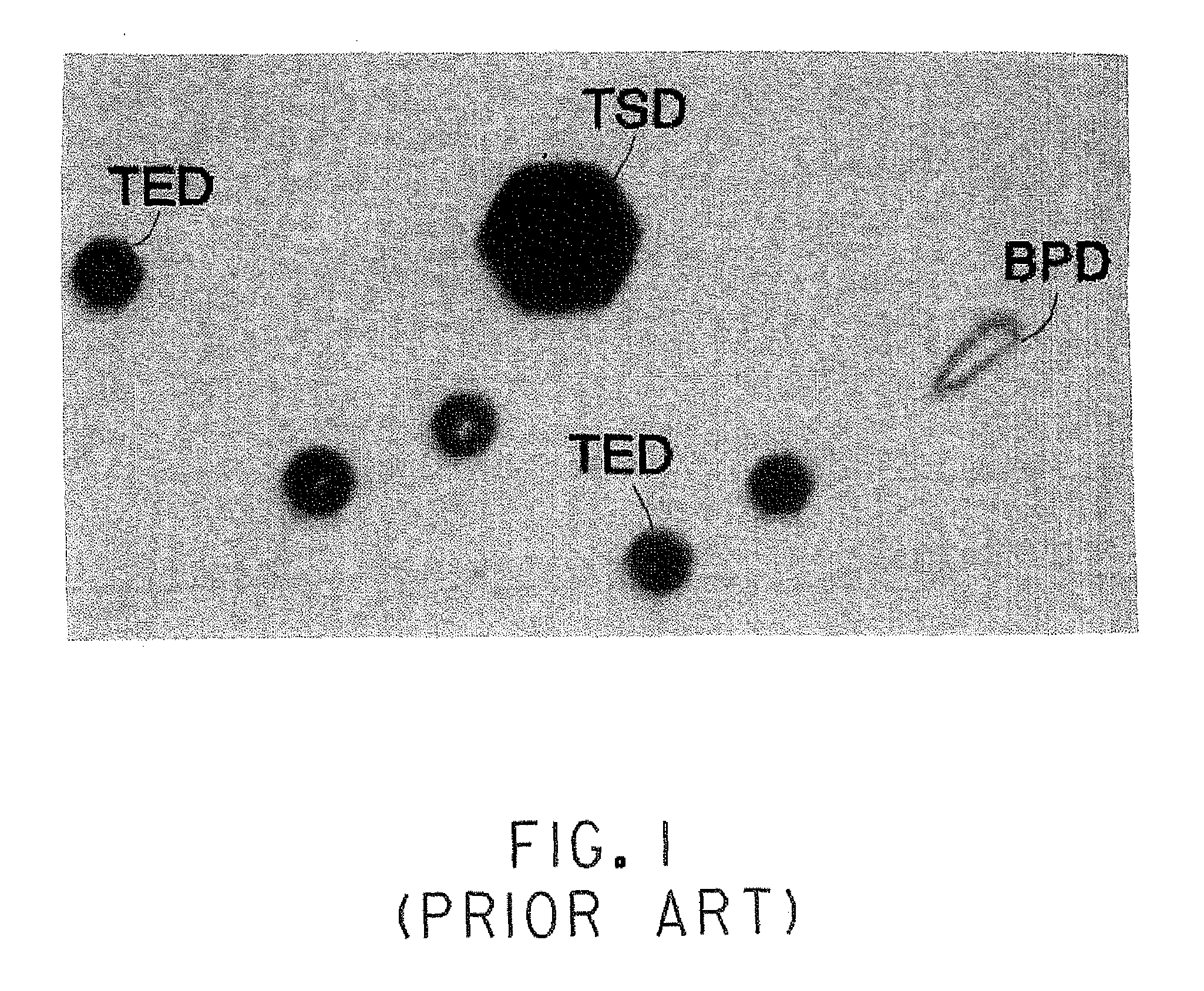
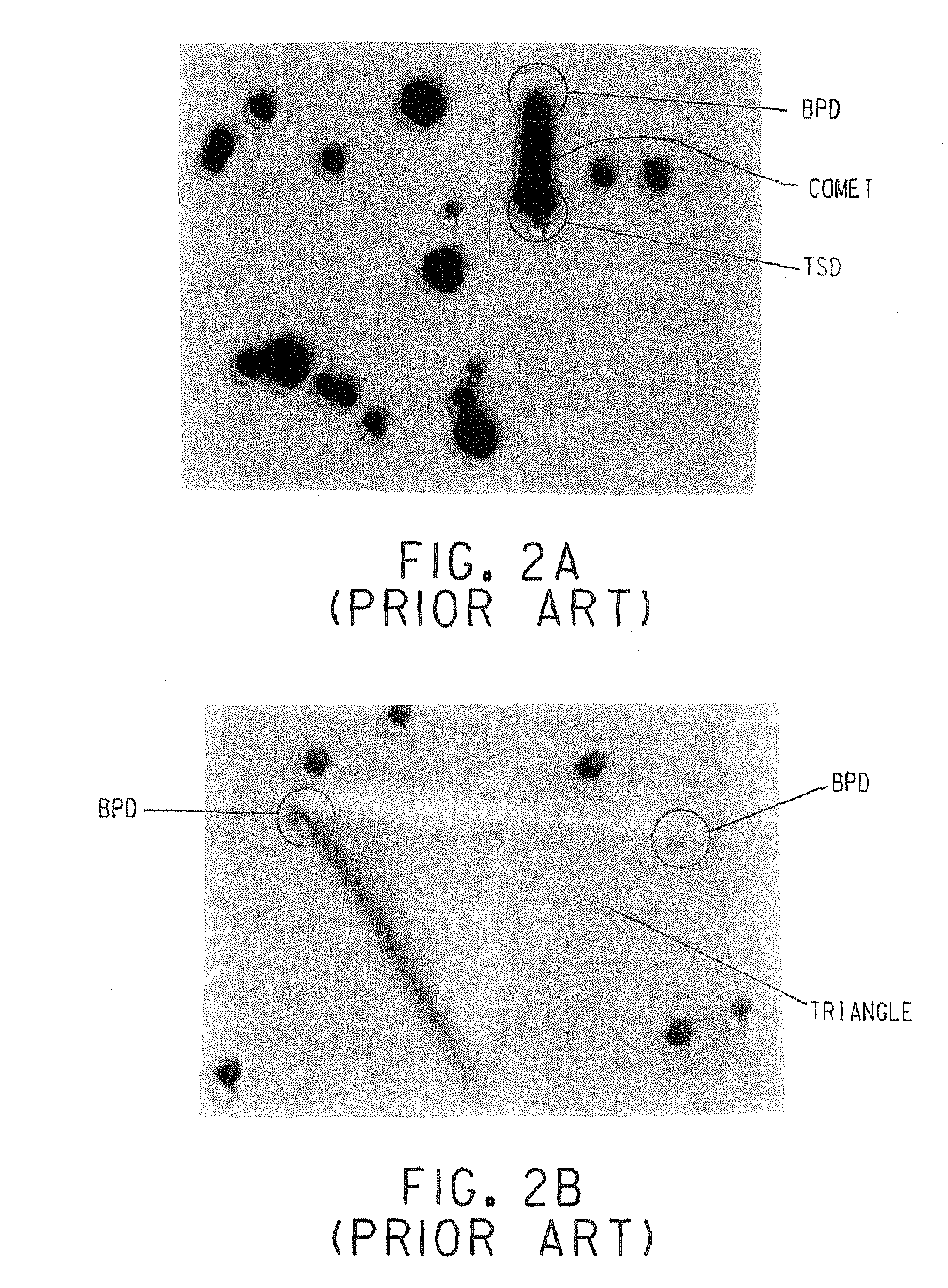
[0041]It has been observed, that sharp perturbations of the SiC single crystal growth process can result in a noticeable reduction in the density of threading dislocations. One desirable way to induce such perturbation is by step-wise doping during growth.

[0042]Step-wise doping creates conditions where adjacent layers of the crystal grown in sequence have slightly different lattice parameters. As a result, a lateral stress component is created which forces each threading dislocation to change the direction of its line in order to avoid or eliminate this stress. Desirably, the direction of each dislocation line changes by 90 degrees, i.e., the dislocation from threading becomes basal. Accordingly, the probability for the dislocation to intersect an opposite sign dislocation located nearby increases. In addition, basal plane dislocat...


PUM


Abstract

In a crystal growth method, a seed crystal 8 and a source material 4 are provided in spaced relation inside of a growth crucible 6. Starting conditions for the growth of a crystal 14 in the growth crucible 6 are then established therein. The starting conditions include: a suitable gas inside the growth crucible 6, a suitable pressure of the gas inside the growth crucible 6, and a suitable temperature in the growth crucible 6 that causes the source material 4 to sublimate and be transported via a temperature gradient in the growth crucible 6 to the seed crystal 8 where the sublimated source material precipitates. During growth of the crystal 14 inside the growth crucible 6, at least one of the following growth conditions are intermittently changed inside the growth crucible 6 a plurality of times: the gas in the growth crucible 6, the pressure of the gas in the growth crucible 6, and the temperature in the growth crucible 6.

Description

BACKGROUND OF THE INVENTION[0001]1. Field of the Invention[0002]The present invention relates to sublimation growth of silicon carbide single crystals with low dislocation density.[0003]2. Description of Related Art[0004]Silicon carbide is an important wide-bandgap material used for the development and manufacturing of SiC and GaN semiconductor devices of new generation. While GaN-based devices are intended for the operation at microwave frequencies, SiC-based devices are aimed at efficient power switching. Other applications are also envisioned and are emerging. Silicon carbide is used as a lattice-matched substrate material to grow epitaxial layers of SiC and GaN. In order to produce low-defect epilayers and high-quality devices, the substrate must have good crystal quality, including low dislocation density.[0005]Dislocations are one-dimensional crystal defects. They are generally categorized based on the value and direction of the so-called Burgers vector, which represents the m...

Claims


Application Information

Patent Timeline
IPC IPC(8): C30B23/02
CPCC30B23/002C30B23/005C30B29/36
Inventor GUPTA, AVINASHCHAKRABARTI, UTPAL K.CHEN, JIHONGSEMENAS, EDWARDWU, PING
Owner II VI
Why Eureka
Try Eureka