Method and apparatus for electroplating including remotely positioned second cathode

a second cathode and electroplating technology, applied in the direction of coatings, electric circuits, manufacturing tools, etc., can solve the problems of increasing the thickness of the deposited copper layer relative to the edge of the wafer, reducing the uniformity of electroplating, and not providing sufficient current redistribution for plating, so as to improve the uniformity of plated layers and improve the effect of uniformity

Active Publication Date: 2010-02-11
NOVELLUS SYSTEMS
View PDF33 Cites 70 Cited by
  • Summary
  • Abstract
  • Description
  • Claims
  • Application Information

AI Technical Summary

Benefits of technology

[0019]The present invention addresses these needs, in one aspect, by providing an apparatus for electroplating a layer of metal on the surface of a wafer which includes a second cathode located remotely with respect to the wafer. The remotely positioned second cathode allows modulation of current density at the wafer surface during an entire electroplating process. In one embodiment, this modulation is achieved by providing a dynamically controlled level of current to the second cathode, where the level of current can be gradually diminished during electroplating process in order to compensate for the diminishing terminal effect. The s

Problems solved by technology

There are several effects, however, that reduce the uniformity of electroplating, leading to increased thickness of deposited copper layer at the edge of the wafer relative to the thickness of copper layer in the center of the wafer.
For example, an electrolyte having sulfuric acid at a concentration of about 10 g/L corresponding to solution conductivity of about 0.05 (ohm-cm)−1 can adequately redistribute current toward the wafer center during electroplating on moderately resistive seed layers that are thicker than about 400 Å. This method alone, however, does not provide sufficient current redistribution for plating on seed layers thinner than 400 Å.
However this method of center-edge distribution control is not normally employed since the additives adsorb on the surface of deposited copper and are incorporated into the electroplated layer thereby altering its properties.
In general, however, small amounts of additives may be useful for improving overall uniformity during electroplating because they increase the interfacial polarization resistance and thus diminish the relative magnitude of the terminal effect.
These shields, however do not adequately improve nonuniformity resulting from terminal effect, since terminal effect is present only in the beginning of electroplating process.
The fixed shields or resistive elements have a constant impact during electroplating process, which can lead to undercompensation of terminal effect during plating on thin seed layers and

Method used


Image

  • Method and apparatus for electroplating including remotely positioned second cathode
  • Method and apparatus for electroplating including remotely positioned second cathode
  • Method and apparatus for electroplating including remotely positioned second cathode

Examples


Embodiment Construction

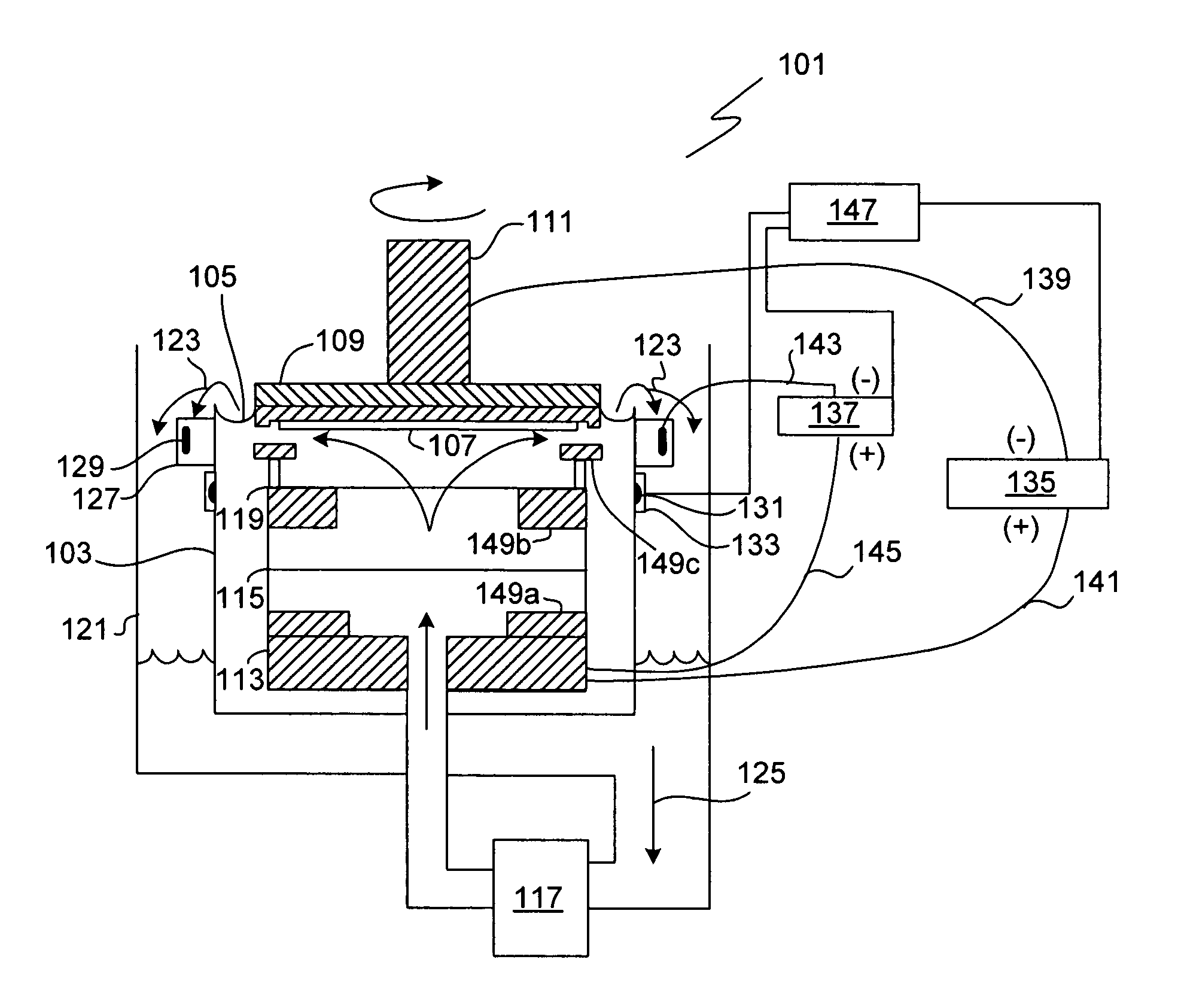
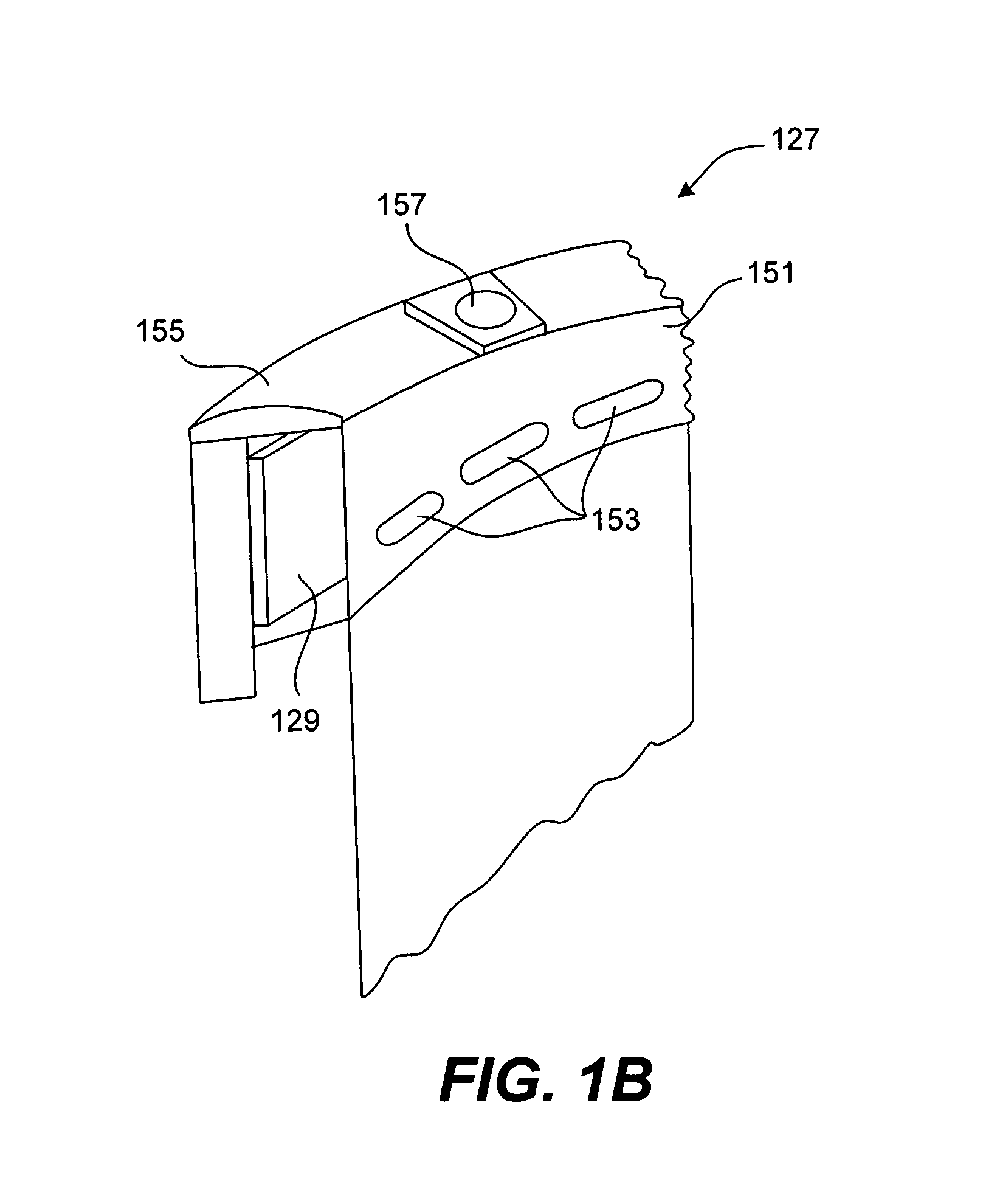
[0035]This invention employs a remotely positioned second cathode, capable of modulating current density at the surface of the wafer. One general advantage of the second cathode is that it allows fine control of the compensating effect by tuning the current or potential at the second cathode. Thus, it is relatively easy to move from providing a large effect at the beginning of the deposition process when the current is carried primary by the seed layer to a smaller effect after some amount of copper has been plated and the terminal effect is diminished. The remote position of this cathode in accordance with embodiments of this invention allows the insulating shields and resistive elements disposed in the plating bath to operate in conjunction with the cathode and shape the current profile experienced by the wafer, and therefore act as a “virtual second cathode”. In a preferred embodiment, the second cathode is disposed outside of the main plating vessel and is separated from the mai...


PUM

PropertyMeasurementUnit
Heightaaaaaaaaaa
Heightaaaaaaaaaa
Thicknessaaaaaaaaaa

Abstract

An apparatus for electroplating a layer of metal on the surface of a wafer includes a second cathode located remotely with respect to the wafer. The remotely positioned second cathode allows modulation of current density at the wafer surface during an entire electroplating process. The second cathode diverts a portion of current flow from the near-edge region of the wafer and improves the uniformity of plated layers. The remote position of second cathode allows the insulating shields disposed in the plating bath to shape the current profile experienced by the wafer, and therefore act as a “virtual second cathode”. The second cathode may be positioned outside of the plating vessel and separated from it by a membrane.

Description

FIELD OF THE INVENTION[0001]The present invention relates generally to a method and apparatus for treating the surface of a substrate and more particularly to a method and apparatus for electroplating a layer on a semiconductor wafer. It is particularly useful for electroplating copper in Damascene and dual Damascene integrated circuit fabrication methods.BACKGROUND OF THE INVENTION[0002]Manufacturing of semiconductor devices commonly requires deposition of electrically conductive material on semiconductor wafers. The conductive material such as copper, is often deposited by electroplating onto a seed layer of metal deposited onto the wafer surface by a PVD or CVD method. Electroplating is a method of choice for depositing metal into the vias and trenches of the processed wafer during Damascene and dual Damascene processing.[0003]Damascene processing is a method for forming interconnections on integrated circuits (IC). It is especially suitable for manufacturing integrated circuits,...

Claims


Application Information

Patent Timeline
IPC IPC(8): C25D21/12C25D17/00C25D7/12C25D5/00
CPCC25D17/002C25D17/001C25D7/123
Inventor REID, JONATHANVARADARAJAN, SESHASAYEEBUCKALEW, BRYANBREILING, PATRICKIBARRETA, GLENN
Owner NOVELLUS SYSTEMS
Why Eureka
Try Eureka