Semiconductor device and a method of manufacturing the same

a semiconductor and capacitor technology, applied in semiconductor devices, capacitors, electrical equipment, etc., can solve the problems of withstand voltage failure between the upper electrode and the lower electrode of the mos capacitor, pin hole defect tends to occur in the capacitor, etc., and achieve the effect of reducing the defect fraction

Inactive Publication Date: 2010-02-11
RENESAS ELECTRONICS CORP
View PDF6 Cites 33 Cited by
  • Summary
  • Abstract
  • Description
  • Claims
  • Application Information

AI Technical Summary

Benefits of technology

[0018]The following describes briefly the effect acquired by the typical invention among the inventions disclosed in the present application.
[0019]It is possible to reduce the fraction defective without the need to perform a screening.

Problems solved by technology

The MOS capacitor and the PIP capacitor are thus formed by lamination, however, it is known that a pin hole defect tends to occur in a capacitor insulating film formed between the upper electrode and the lower electrode particularly in the MOS capacitor, which is formed in the lower layer.
That is, if a pin hole defect occurs in a capacitor insulating film, a withstand voltage failure between the upper electrode and the lower electrode constituting the MOS capacitor becomes a problem.

Method used


Image

  • Semiconductor device and a method of manufacturing the same
  • Semiconductor device and a method of manufacturing the same
  • Semiconductor device and a method of manufacturing the same

Examples


first embodiment

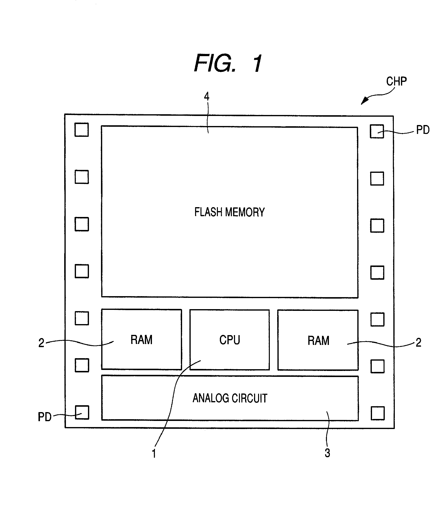
[0059](First embodiment) FIG. 1, for example, is a plan view showing a semiconductor chip (semiconductor substrate) CHP that forms a microcomputer, and a diagram showing a layout configuration of each element formed in the semiconductor chip CHP. In FIG. 1, the semiconductor chip CHP has a CPU (Central Processing Unit) 1, a RAM (Random Access Memory) 2, an analog circuit 3, and a flash memory 4. Then, on the periphery of the semiconductor chip, pads PD that are input / output external terminals to couple these circuits and external circuits are formed.

[0060]The CPU (circuit) 1 is also called a central processing unit and plays an important role as the heart of a computer etc. The CPU 1 reads and decodes a command from a storage device and performs a variety of operations and controls based thereon and high-speed of processing is required. Consequently, a MISFET (Metal Insulator Semiconductor Field Effect Transistor) constituting the CPU 1 requires a relatively larger current drive for...

second embodiment

[0188]FIG. 25 is a plan view showing a connection configuration of capacitive elements in the On the left-hand side in FIG. 25, a first capacitance formation region is formed and on the right-hand side in FIG. 25, a second capacitance formation region is formed. In the first capacitance formation region formed on the left-hand side in FIG. 25, a capacitive element having a laminated structure of the MOS capacitor MOS1 and the polysilicon capacitor PIP1 is formed. Although an n-type well, which is the lower electrode of the MOS capacitor MOS1, is not seen, the n-type semiconductor region MV formed in this n-type well is shown schematically. On the other hand, in the second capacitance formation region formed on the right-hand side in FIG. 25, a capacitive element having a laminated structure of the MOS capacitor MOS2 and the polysilicon capacitor PIP2 is formed. Although a p-type well, which is the lower electrode of the MOS capacitor MOS2, is not seen, a p-type semiconductor region...

third embodiment

[0207](Third embodiment) The third embodiment is the same as the above-described second embodiment in that an n-type well with a low concentration is used as the lower electrode of the MOS capacitor MOS1 and a p-type well with a low concentration is used as the lower electrode of the MOS capacitor MOS2, however, differs from the second embodiment in the configuration of a drawn region drawn from the respective lower electrodes.

[0208]FIG. 32 is a plan view showing a connection configuration of capacitive elements in the third embodiment. On the left-hand side in FIG. 32, a first capacitance formation region is formed and on the right-hand side in FIG. 32, a second capacitance formation region is formed. In the first capacitance formation region formed on the left-hand side in FIG. 32, a capacitive element having a laminated structure of the MOS capacitor MOS1 and the polysilicon capacitor PIP1 is formed. Although an n-type well, which is the lower electrode of the MOS capacitor MOS1,...


PUM


Abstract

A technology capable of reducing the fraction defective of a MOS capacitor without the need to perform a screening is provided.
A MOS capacitor MOS1 and a MOS capacitor MOS2 are coupled in series between a high potential and a low potential to form a series capacitive element. Then, a polysilicon capacitor PIP1 and a polysilicon capacitor PIP2 are coupled in parallel with the series capacitive element. Specifically, a high-concentration semiconductor region HS1 constituting a lower electrode of the MOS capacitor MOS1 and a high-concentration semiconductor region HS2 constituting a lower electrode of the MOS capacitor MOS2 are coupled. Further, an electrode E1 constituting an upper electrode of the MOS capacitor MOS1 is coupled to the low potential (for example, GND) and an electrode E3 constituting an upper electrode of the MOS capacitor MOS2 is coupled to the high potential (for example, power source potential).

Description

CROSS-REFERENCE TO RELATED APPLICATION[0001]The disclosure of Japanese Patent Application No. 2008-202554 filed on Aug. 6, 2008 including the specification, drawings and abstract is incorporated herein by reference in its entirety.BACKGROUND OF THE INVENTION[0002]The present invention relates to a semiconductor device and its manufacturing technology and, more particularly, to a semiconductor device including a plurality of capacitive elements and a technology effective when applied to its manufacture.[0003]In Japanese patent laid-open No. 2003-60042 (patent document 1), a technology is described, which forms a capacitive element (capacitor) by laminating it over a semiconductor substrate. Specifically, a structure is disclosed, which is formed by laminating a MOS (Metal Oxide Semiconductor) capacitor including a well (first electrode) formed in the semiconductor substrate and a second electrode including a polysilicon film formed over the well via an insulating film and a PIP (Poly...

Claims


Application Information

Patent Timeline
Patent Type & Authority Applications(United States)
IPC IPC(8): H01L27/105H01L21/02H01L21/8234H01L29/92
CPCH01L21/28273H01L27/11526H01L27/11546H01L29/94H01L29/42344H01L29/792H01L28/40H01L29/40114H10B41/40H10B41/49
Inventor UENO, MAYA
Owner RENESAS ELECTRONICS CORP
Why Eureka
Try Eureka