Wavelength selection method, film thickness measurement method, film thickness measurement apparatus, and system for producing thin film silicon device

a thin film, wavelength selection technology, applied in the direction of measurement devices, instruments, coatings, etc., can solve the problems of inability to measure with the desired accuracy, the measurement error is larger than an acceptable range, and the film thickness monitoring accuracy cannot be improved, so as to improve power generation efficiency, yield, and production efficiency.

Inactive Publication Date: 2010-02-11
MITSUBISHI HEAVY IND LTD
View PDF2 Cites 25 Cited by
  • Summary
  • Abstract
  • Description
  • Claims
  • Application Information

AI Technical Summary

Benefits of technology

[0031]The present invention is effective in reducing the film thickness measurement error. In addition, since the variation in film thickness can be monitored, the present invention is effective in improving the power generation efficiency, yield, and production efficiency.

Problems solved by technology

However, in the film thickness measurement disclosed in Patent Document 1, it was found that, when evaluating the thicknesses of thin films which are formed on different substrates or which have different surface irregularities, variations occur in the amount of transmitted light, and the measurement result may in some cases contain a measurement error larger than an acceptable range.
In addition, due to this error, there has been a problem in that the thickness cannot be measured with the desired accuracy, and as a result, film-thickness monitoring accuracy cannot be improved.
In addition, when a film thickness meter exclusively used for thin-film thickness measurement (such as a spectral ellipsometer or a spectrophotometer) is used, a substrate in a production line must be temporarily removed for measurement and evaluation, and it takes time to obtain measurement results; hence, there has been a problem in that all products cannot be monitored online during production.

Method used


Image

  • Wavelength selection method, film thickness measurement method, film thickness measurement apparatus, and system for producing thin film silicon device
  • Wavelength selection method, film thickness measurement method, film thickness measurement apparatus, and system for producing thin film silicon device
  • Wavelength selection method, film thickness measurement method, film thickness measurement apparatus, and system for producing thin film silicon device

Examples


first embodiment

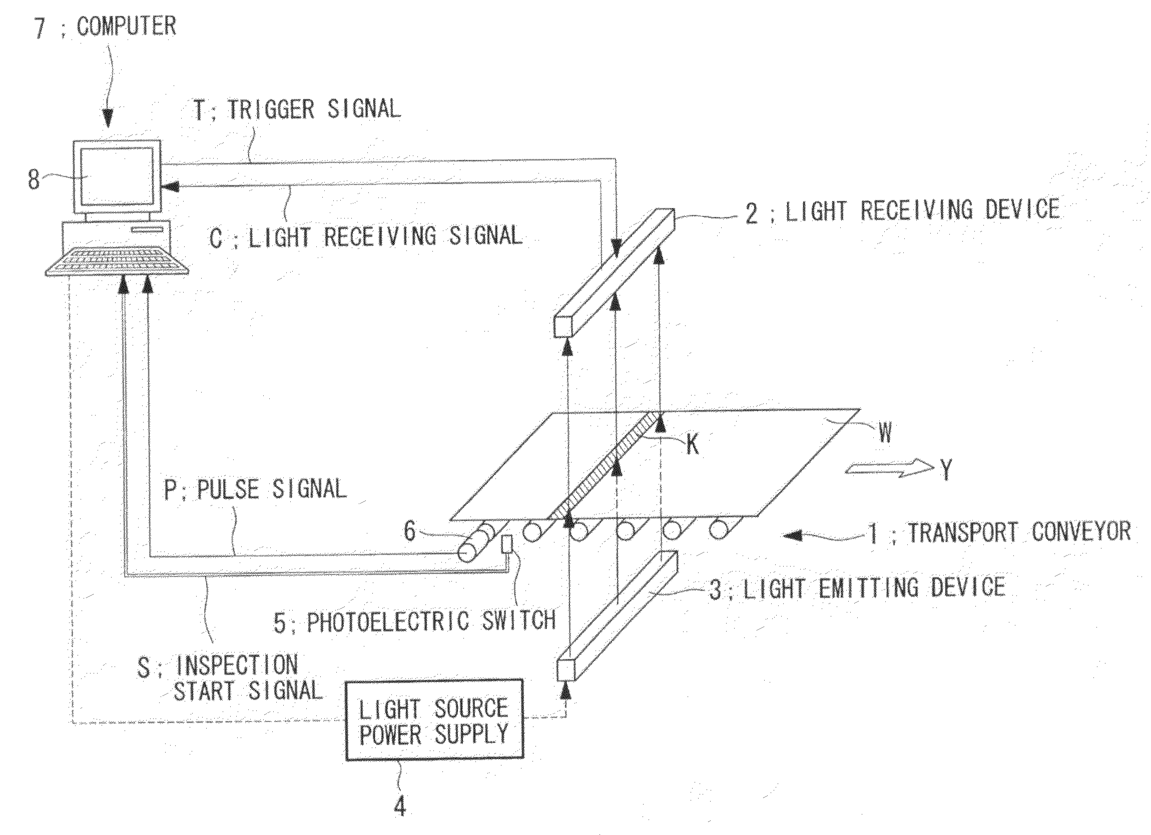
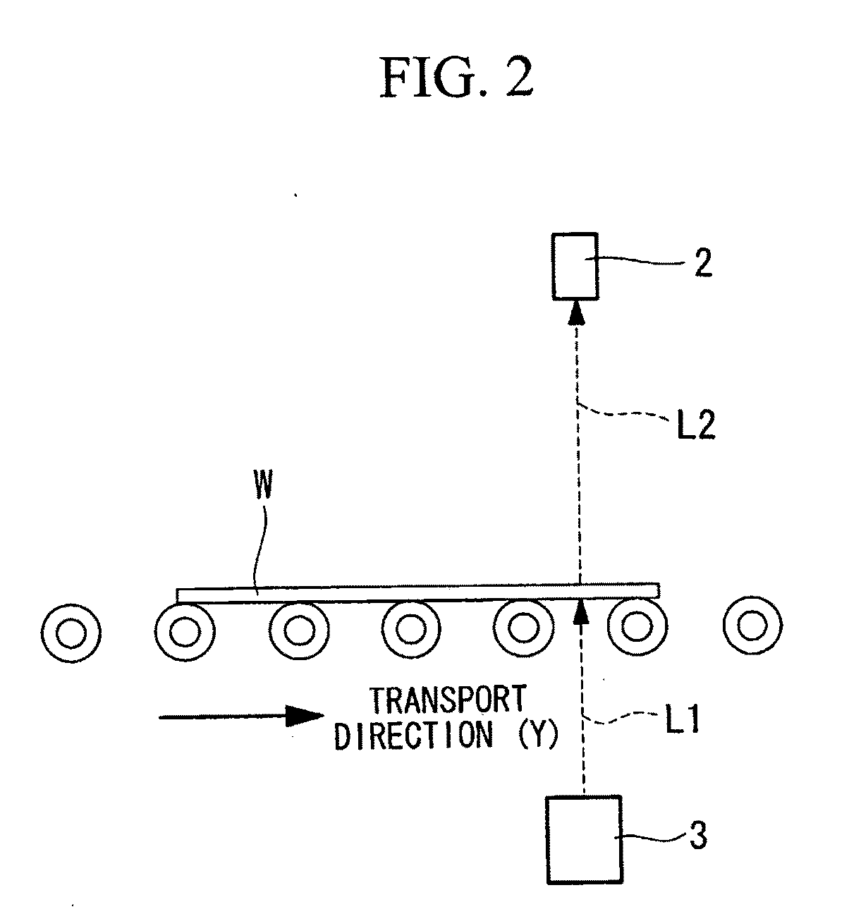
[0048]FIG. 1 is a view showing the entire structure of a thin-film thickness measurement apparatus according to the first embodiment of the present invention.

[0049]In the film thickness measurement apparatus shown in FIG. 1, a substrate W is transported in a transport direction (Y direction in the figure) by a transport conveyor 1. This substrate W is composed, for example, of a transparent conductive film formed by a thermal CVD apparatus and a crystalline silicon film photoelectric conversion layer formed by a plasma CVD apparatus, formed in that order on a transparent glass substrate. Alternatively, this substrate W is composed of a transparent conductive film formed by a thermal CVD apparatus, an amorphous silicon film photoelectric conversion layer formed by a plasma CVD apparatus, and a crystalline silicon film photoelectric conversion layer formed by a plasma CVD apparatus, formed in that order on a transparent glass substrate. Alternatively, this substrate W is composed of a...

second embodiment

[0081]Next, a film thickness measurement apparatus according to a second embodiment of the present invention will be described.

[0082]In the film thickness measurement of a thin film, besides the crystallinity described above, the measurement error is caused by surface irregularities of the thin film. Accordingly, in order to reduce the measurement error caused by surface irregularities, the wavelength of illumination light is selected.

[0083]In this embodiment, a plurality of samples having different thicknesses and different degrees of surface irregularity is prepared. In order to evaluate the degree of surface irregularity of a microcrystalline silicon film, a haze ratio is used. The haze ratio is represented by diffused transmitted light / total transmitted light and is measured, for example, by a known haze meter (such as HR-100 manufactured by Murakami Color Research Laboratory, in accordance with ASTM D-1003).

[0084]The surface irregularity of the microcrystalline silicon film is ...


PUM


Abstract

An object is to reduce film thickness measurement error. Illumination light having different wavelengths is radiated onto a plurality of samples in which thin films having different film qualities and film thicknesses are provided on substrates, evaluation values related to the amounts of transmitted light when the illumination light of each wavelength is radiated are measured, film thickness characteristics, showing the relationship between the evaluation values and the film thicknesses for each film quality, are formed at each wavelength based on the measurement results, and among the film thickness characteristics, a wavelength at which a measurement difference between the evaluation values caused by the film qualities is in a predetermined range is selected.

Description

TECHNICAL FIELD[0001]The present invention relates to film thickness measurement of a thin film, and more particularly relates to a wavelength selection method for selecting a wavelength to be used for film thickness measurement of a thin film including a crystalline silicon film formed on a substrate of a thin film silicon device, to a film thickness measurement method for performing film thickness measurement using a wavelength selected by the above wavelength selection method, to an apparatus for the film thickness measurement method, and to a system for producing a thin film silicon device including a thin-film formation process.BACKGROUND ART[0002]Heretofore, a technique for measuring the thickness of a thin film formed on a light-transmissive substrate by using optical absorption characteristics of a material has been known (for example, see Patent Document 1).[0003]Patent Document 1 discloses a technique in which, in a production line of thin film solar cells, light is radiat...

Claims


Application Information

Patent Timeline
Patent Type & Authority Applications(United States)
IPC IPC(8): G01B11/06
CPCG01B11/0633G01B11/303G01B11/0683G01B2210/46
Inventor SAKAI, SATOSHIIIDA, MASAMIKAWAZOE, KOHEI
Owner MITSUBISHI HEAVY IND LTD
Why Eureka
Try Eureka