

CVD Device with Substrate Holder with Differential Temperature Control
a technology of temperature control and substrate, applied in the direction of chemically reactive gases, coatings, crystal growth processes, etc., can solve the problems of affecting the growth characteristics of layers, affecting the growth of layers, and affecting the surface radiation loss, etc., to achieve the effect of reducing the dimensions of the substrate bearing disk, and reducing the risk of damag
- Summary
- Abstract
- Description
- Claims
- Application Information
AI Technical Summary
Benefits of technology
Problems solved by technology
Method used
Image

Examples
Embodiment Construction
[0022]Referring now to the drawings, wherein like reference numerals designate corresponding structure throughout the views.
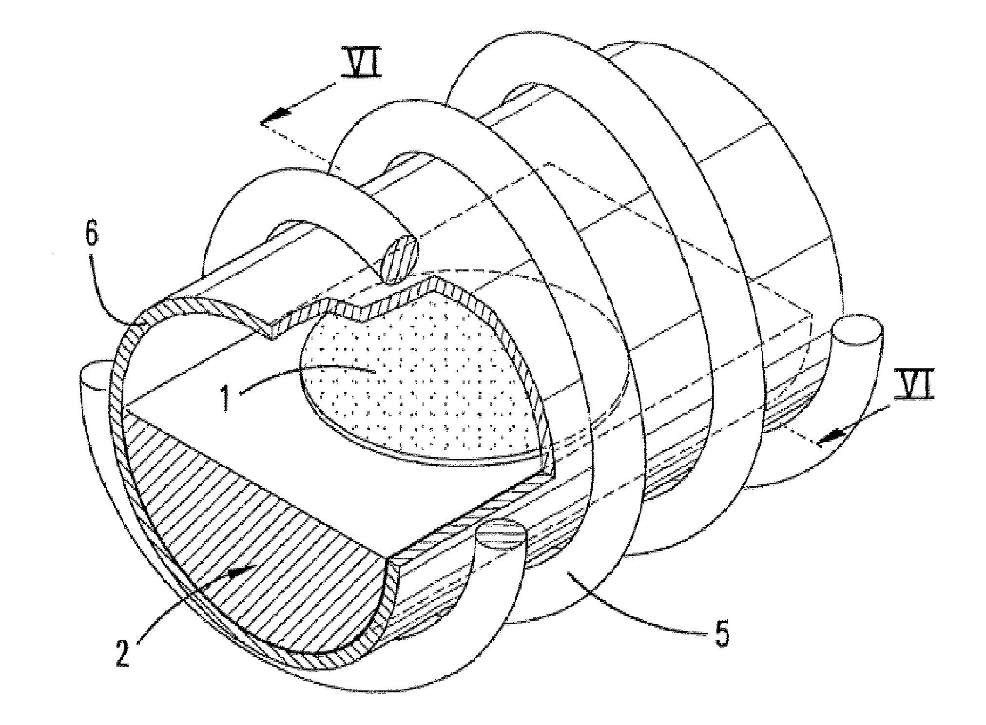
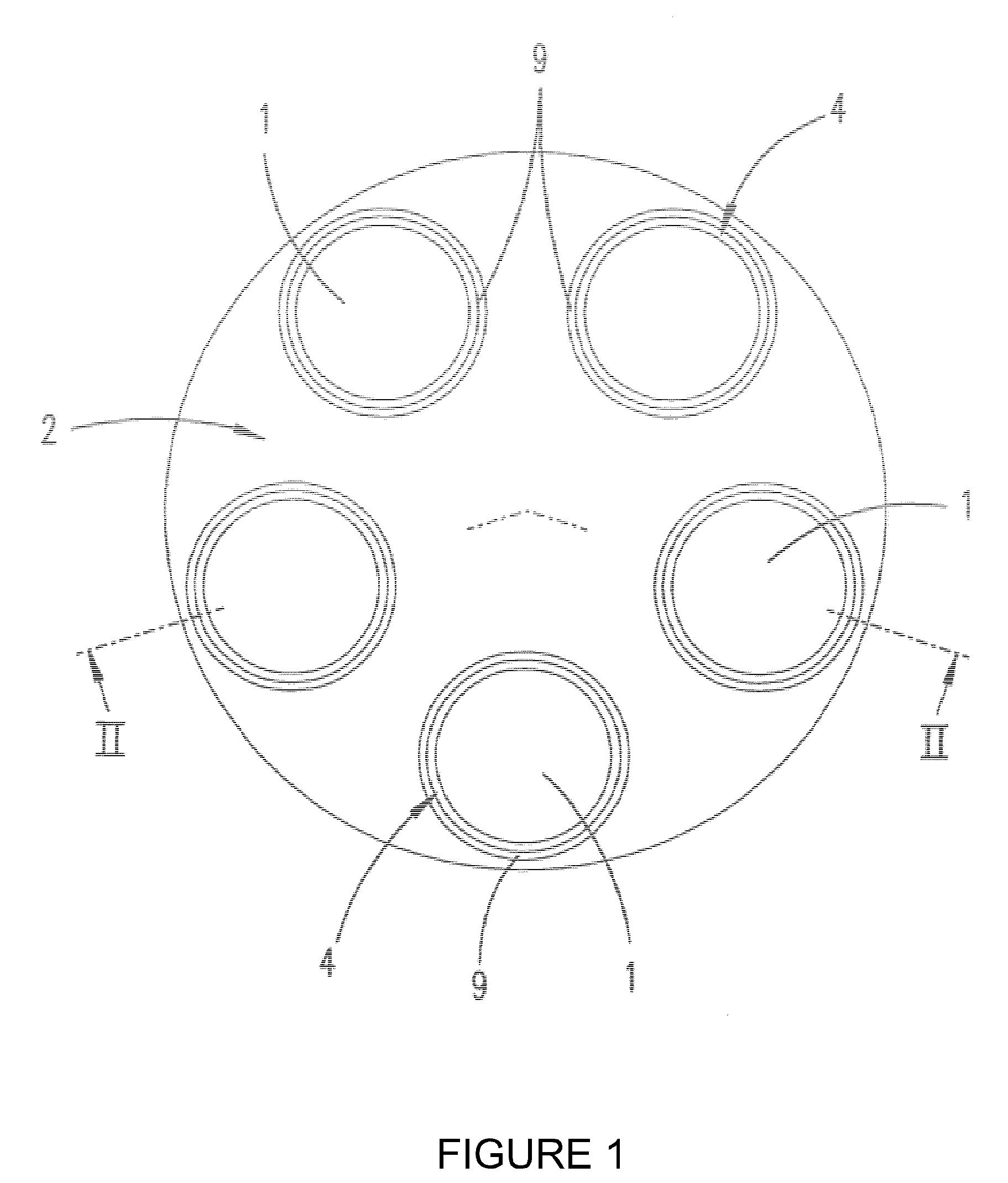
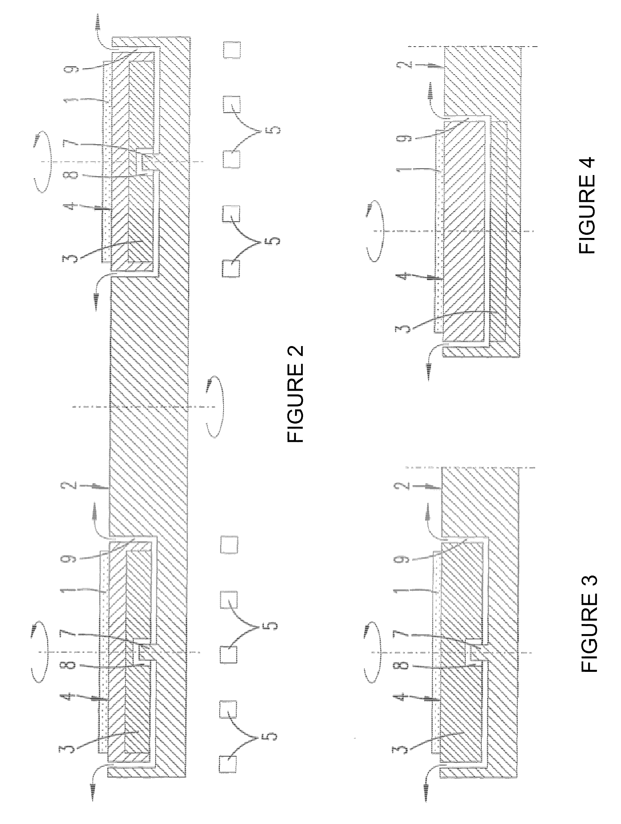
[0023]The substrate holder 2 illustrated in FIGS. 1-4 comprises a block of graphite which is in the form of a cylindrical disk and is located in a reactor, driven in rotation about its own axis. The reactive gases are introduced into the process chamber through a feed line disposed above and in the center of the substrate holder. The walls of this process chamber are not heated. They are only heated by the radiation of the substrate holder 2, which is heated from below by means of an HF coil 5. The result of this is that there is a temperature drop inside the process chamber from the substrate holder 2 toward the process chamber walls (not shown). The reactive gases which are introduced into the process chamber and which may be trimethyl-gallium, trimethyl-indium, arsine and / or phosphine, partially decompose in the gas phase and on the substrate surface. On the...
PUM
| Property | Measurement | Unit |
|---|---|---|
| surface area | aaaaa | aaaaa |
| electrical conductivity | aaaaa | aaaaa |
| surface temperature | aaaaa | aaaaa |
Abstract
Description
Claims
Application Information