
Eureka
For R&D, Eureka makes reading and utilizing patents & technical documents easy.
Eureka AIR
Designed for self-driven R&D workflows. Generate viable solutions, solve complex R&D challenges, empower your innovation with AI.

Eureka Materials
Designed for material experts only. Revolutionize your material R&D, from search, analyze, to developing new materials.

TechResearch
Generate reliable direction feasibility study reports for your R&D in just a few steps.

TechSeek
Discover and master advanced knowledge NOW. Basics, ideas, possibilities, all at once.

TechMind
As an expert in R&D Theories, TechMind can generates customized viable solutions instantly.

TechRisk
Analyze your overall solution with one click, know your potential R&D risks in advance.

TechMonitor
Get weekly tech updates, stay abreast of the latest tech innovations and key insights.
Annealing apparatus
- Summary
- Abstract
- Description
- Claims
- Application Information
AI Technical Summary
Benefits of technology
Problems solved by technology
Method used
Image

Examples
Embodiment Construction
[0040]Hereinafter, embodiments of the invention will be described with reference to the accompanying drawings. An annealing apparatus for annealing a wafer of which surface is implanted with impurities will be described herein by way of example.
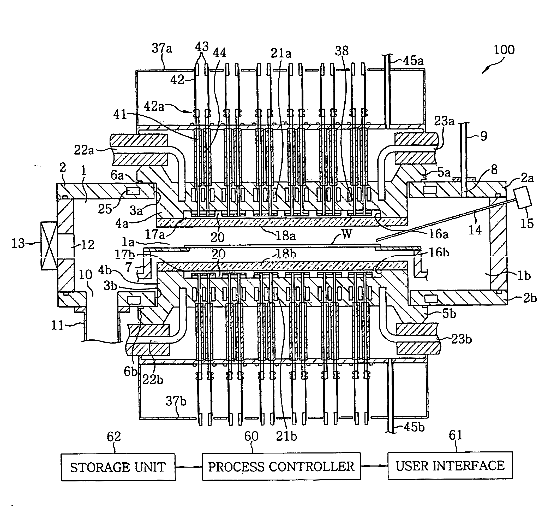
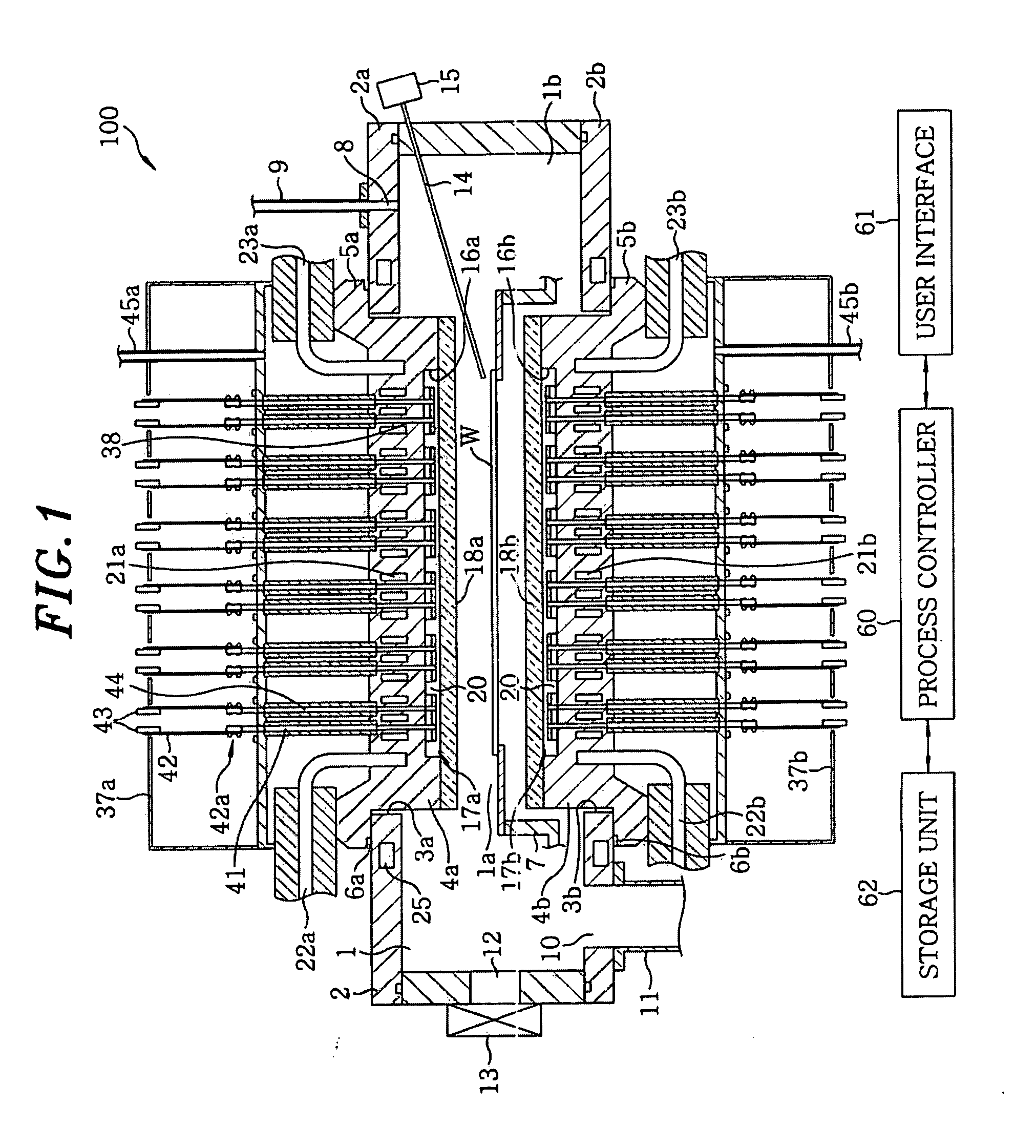
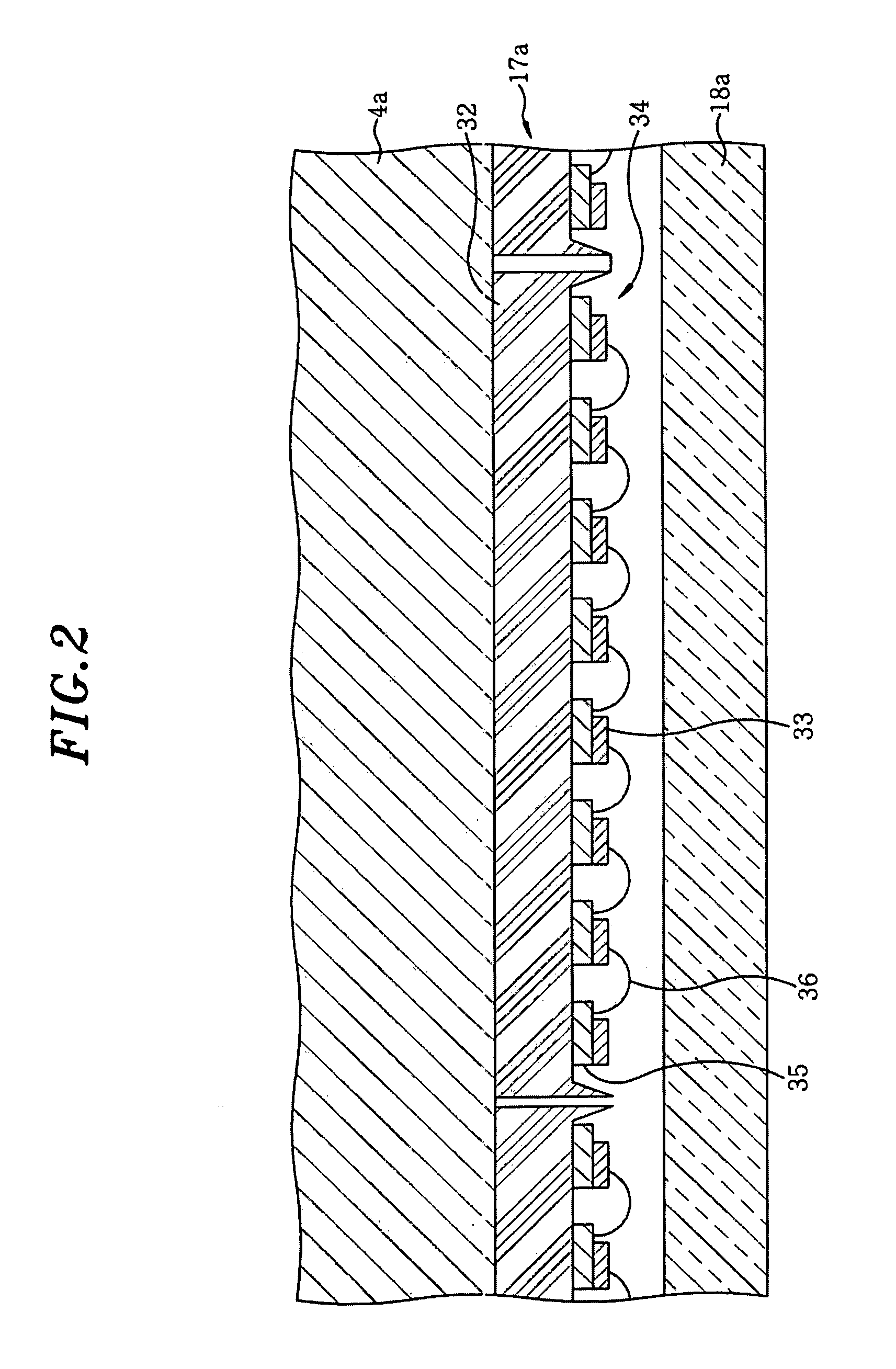
[0041]FIG. 1 is a sectional view showing a schematic configuration of an annealing apparatus in accordance with the embodiment of the present invention. FIG. 2 is an enlarged sectional view illustrating a heating source of the annealing apparatus shown in FIG. 1. FIG. 3 is an enlarged sectional view illustrating the portion through which to supply a power to LEDs of the annealing apparatus shown in FIG. 1. The annealing apparatus 100 includes an airtightly sealed processing chamber 1 into which a wafer W is loaded.
[0042]The processing chamber 1 has a cylindrical annealing portion 1a in which the wafer W is positioned and a gas diffusing portion 1b formed in a doughnut shape outside the annealing portion 1a. The gas diffusing portion 1b is gre...
PUM
| Property | Measurement | Unit |
|---|---|---|
| Power | aaaaa | aaaaa |
| Transparency | aaaaa | aaaaa |
| Thermal conductivity | aaaaa | aaaaa |
Abstract
Description
Claims
Application Information
 - R&D Engineer
- R&D Manager
- IP Professional
- Industry Leading Data Capabilities
- Powerful AI technology
- Patent DNA Extraction
Browse by: Latest US Patents, China's latest patents, Technical Efficacy Thesaurus, Application Domain, Technology Topic, Popular Technical Reports.
© 2024 PatSnap. All rights reserved.Legal|Privacy policy|Modern Slavery Act Transparency Statement|Sitemap|About US| Contact US: help@patsnap.com