[0015]The above mentioned and other technical contents, characteristics, and effects of the invention can be illustrated more clearly by the following detailed descriptions together with the corresponding figures. The wording describing directions used in the following descriptions, such as: up, down, left, right, front, back or the like, indicates the directions with respect to the figure only. Therefore, the wording used to describe directions is for illustration but not to limit the scope of the invention.
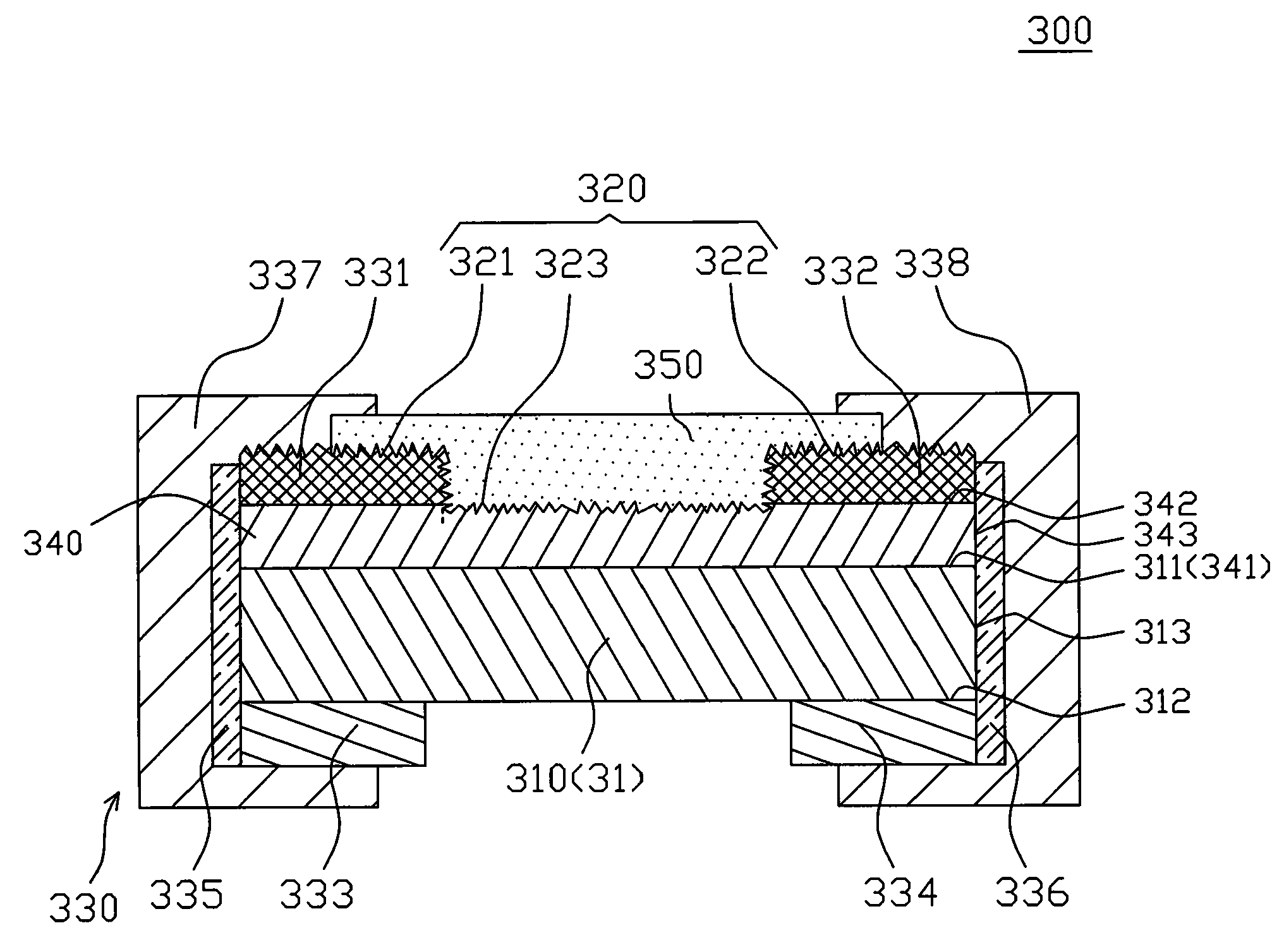
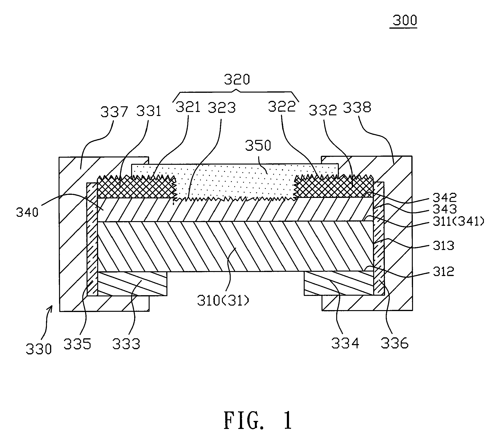
[0016]FIG. 1 shows a cross sectional view of a resistive component 300 according to one embodiment of the invention. The resistive component 300 is suitable for detecting electric current in a circuit and has a
low resistance value and a low
temperature coefficient of resistance (TCR). Preferably, its resistance value is lower than about 10 mΩ and its TCR is lower than about 100×10−6 / K (ppm / K).
[0017]The resistive component 300 comprises a carrier 31, a resistive layer 340, an
electrode unit 330, an upper oxide layer 320, and a protective layer 350. The carrier 31 includes a substrate 310. The substrate 310 is made of insulating material having a good thermal conducting property, such as the
alumina (Al2O3). The substrate 310 includes an upper surface 311, a lower surface 312 opposite to the upper surface 311, and a side surface 313 connecting the upper surface 311 and the lower surface 312.
[0018]The resistive layer 340 is disposed on the upper surface 311 of the substrate 310 and comprises
copper alloy. The
copper alloy is either
nickel copper alloy whose
nickel and copper are main compositions or
manganese copper
alloy whose
manganese and copper are main compositions. The resistive layer 340 can be formed onto the substrate 310 directly by the thin film process, such as the
sputtering or the evaporating
deposition process. The resistive layer 340 includes a first surface 341, a second surface 342 opposite to the first surface 341, and a side surface 343 connecting the first surface 341 and the second surface 342. The first surface 341 is disposed on the upper surface 311 of the substrate 310. In this embodiment, the thickness of the resistive layer 340 is about between 0.2 mm and 0.6 mm.
[0019]The electrode unit 330 comprises a pair of upper electrodes 331&332. The upper electrodes 331&332 are electrically connected to the resistive layer 340 but are mutually separated from each other. In this embodiment, the upper electrodes 331&332 can be the conductive bumps disposed respectively on the two sides of the second surface 342 of the resistive layer 340 to cover a part of the second surface 342 of the resistive layer 340. The upper electrodes 331&332 can be made of copper.
[0020]The upper oxide layer 320 is disposed directly on a part of the second surface 342 of the resistive layer 340 and on the surfaces, away from the resistive layer 340, of the upper electrodes 331&332. The upper oxide layer 320 is a roughened surface formed by performing oxidation treatment, in which a wet
etching process is used, on a part of the resistive layer 340 and a part of the upper electrode
layers 331&332. More specifically, an embodiment of the invention can utilize brown or black oxidation treatment. Preferably, the brown oxidation treatment is used to form the upper oxide layer 320 made of copper alloy oxide so that the resistivity of the upper oxide layer 320 is substantially the same as that of the resistive layer 340. The centerline average roughness (Ra) of the roughened surface is about 1100±500 Å, that is about between 600 Å and 1600 Å. In this embodiment, the upper oxide layer 320 comprises a first oxide layer 321 that covers the upper electrode 331, a second oxide layer 322 that covers the upper electrode 332, and a third oxide layer 323 that covers the portion of the second surface 342 of the resistive layer 340 which is not disposed with the upper electrodes 331&332. The thickness of the upper oxide layer 320 is set to be about between 40 μm and 100 μm, which is far less than the thickness of the resistive layer 340, so that the variance of the
temperature coefficient of resistance of the resistive component can be reduced. Part of the material composition of the upper oxide layer 320 comprises at least the oxide of the resistive layer 340. More specifically, the first oxide layer 321 and the second oxide layer 322 comprise, at least, the oxide of the upper electrodes 331&332 while the third oxide layer 323 comprises, at least, the oxide of the resistive layer 340.

