Capacitance evaluation circuit and electronic device using the same
a technology of capacitive evaluation and circuit, which is applied in the direction of testing circuit, pulse technique, instruments, etc., can solve the problem that the conventional mechanical device tends to have the structural damage during the user's operation process
- Summary
- Abstract
- Description
- Claims
- Application Information
AI Technical Summary
Benefits of technology
Problems solved by technology
Method used
Image
Examples
first embodiment
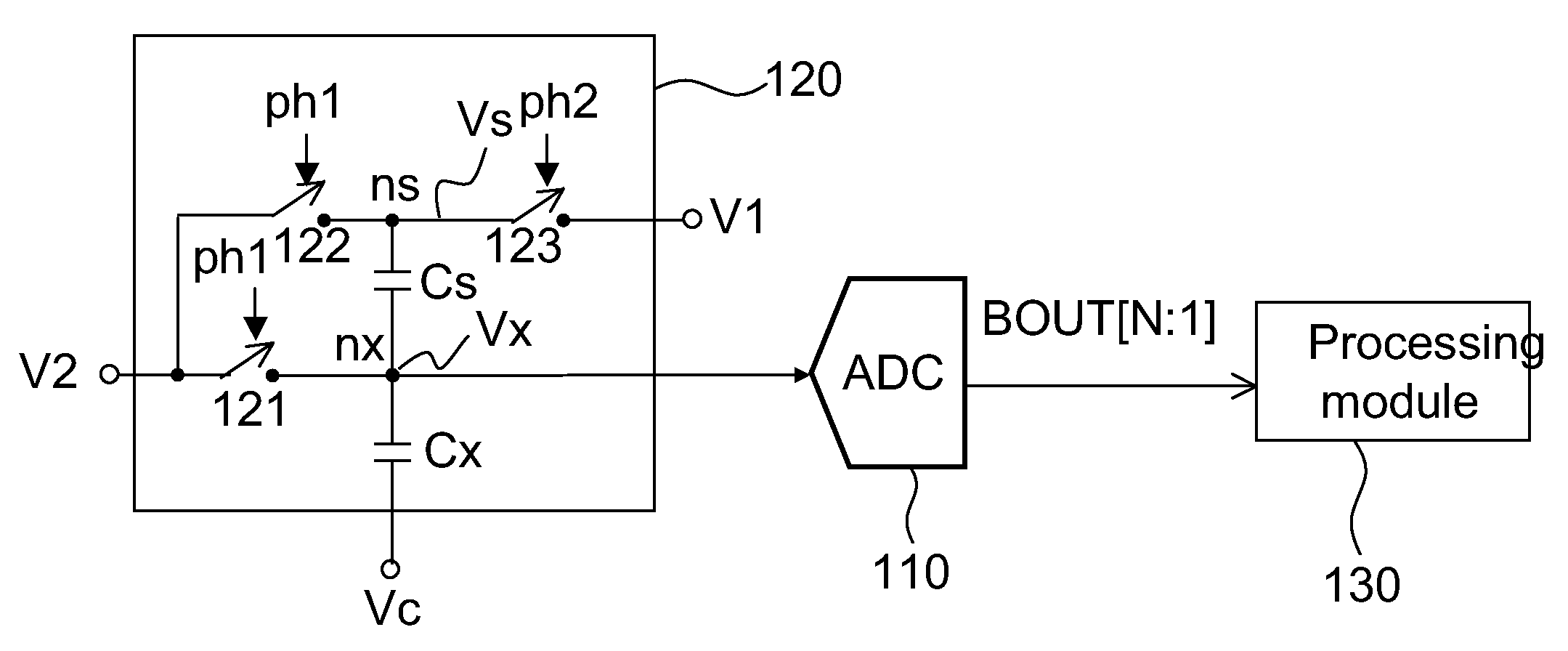
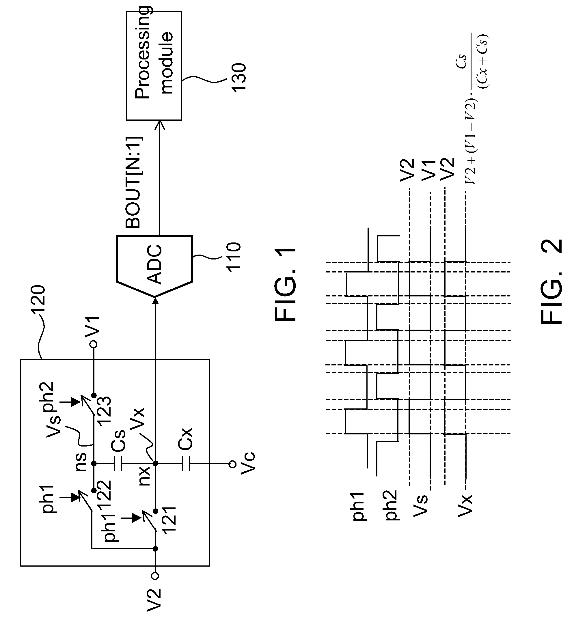
[0019]FIG. 1 is a schematic illustration showing a capacitance evaluation circuit according to a first embodiment of the invention. FIG. 2 shows associated waveforms of FIG. 1.
[0020]Referring to FIG. 1, the capacitance evaluation circuit includes an ADC 110, a capacitive voltage divider 120 and a processing module 130. The ADC 110 has, for example, a sigma-delta ADC with a sample-hold (S / H) function. The capacitive voltage divider 120 includes switches 121 to 123, and capacitors Cs and Cx. In this embodiment, V1, V2 and Vc are voltage sources. It is assumed that V12, and a clock signal ph1 is an inverse of a clock signal ph2.
[0021]The switch 121 has one terminal coupled to the voltage source V2, and the other terminal coupled to a node nx. The voltage of the node nx is Vx. The conduction state of the switch 121 is controlled by the clock signal ph1. For example, the switch 121 is turned on when the clock signal ph1 has the high potential; and vice versa. When the switch 121 is turne...
second embodiment
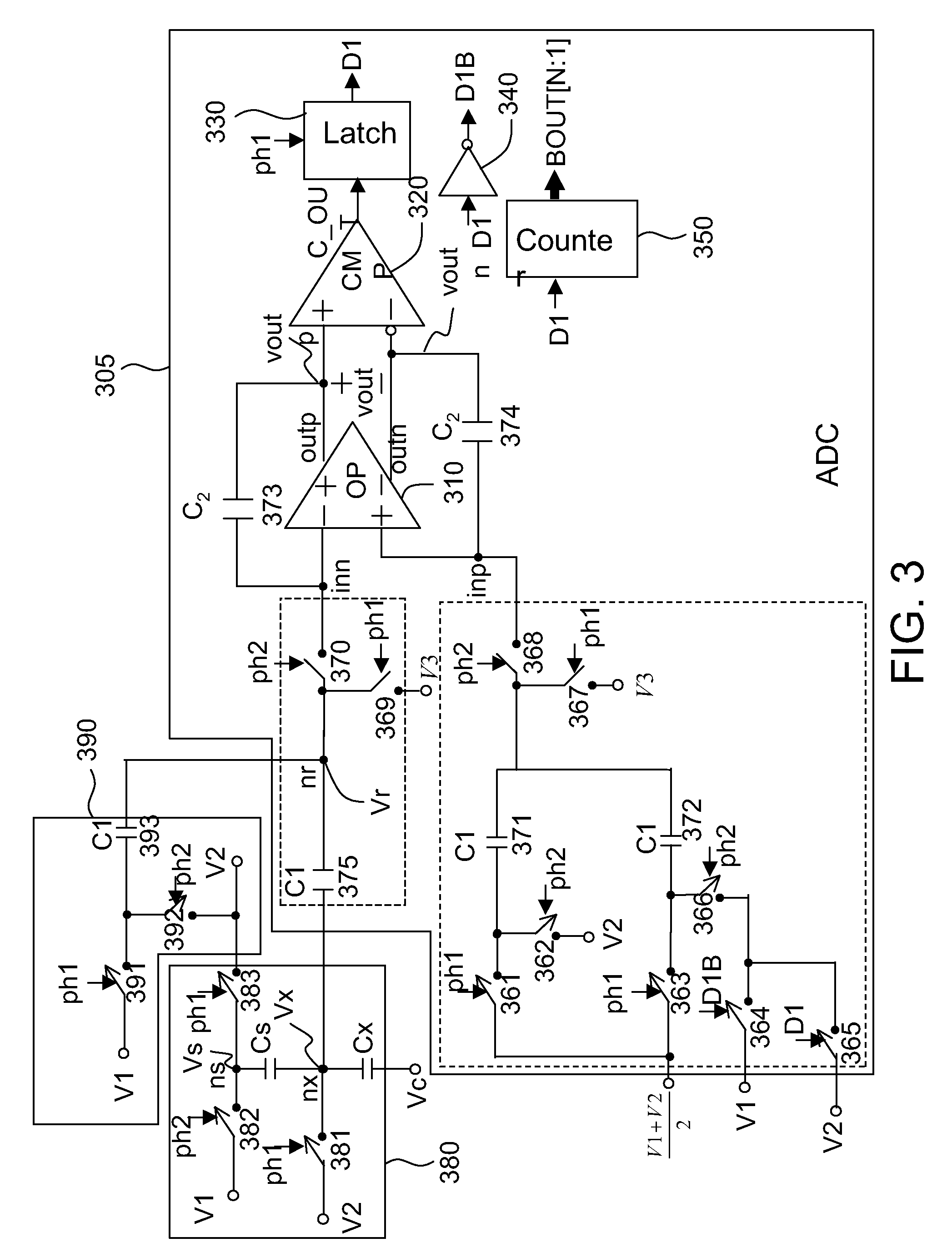
[0035]FIG. 3 is a schematic illustration showing a capacitance evaluation circuit according to a second embodiment of the invention. FIG. 4 shows associated waveforms of FIG. 3.
[0036]As shown in FIG. 3, the capacitance evaluation circuit includes an ADC 305, a capacitive voltage divider 380 and a bias circuit 390. For example, the ADC 305 is a sigma-delta ADC having the sample-hold (S / H) function.
[0037]The ADC 305 includes an operation amplifier (OP) 310, a comparator (CMP) 320, a latch 330, an inverter 340, a counter 350, switches 361 to 370 and capacitors 371 to 375.
[0038]The operation amplifier 310 has a positive input terminal inp coupled to the switch 368 and the capacitor 374; a negative input terminal inn coupled to the switch 370 and the capacitor 373; a positive output terminal outp coupled to a positive input terminal of the comparator 320 and the capacitor 373; and a negative output terminal outn coupled to a negative input terminal of the comparator 320 and the capacitor...
third embodiment
[0088]FIG. 5 is a schematic illustration showing function blocks of an electronic device according to a third embodiment of the invention. The electronic device includes, for example but without limitation to, a digital camera having a touch screen. The electronic device includes a sensor 510, a multiplexer 520 and an ADC 530.
[0089]The sensor 510 includes, for example but without limitation to, a photosensor, a tilt sensor, a temperature sensor and a humidity sensor. The sensor 510 may sense the external environment and converts the sensed data into the analog voltage. The analog voltage is converted into the digital signal through the ADC 530, and then a post-end processing module determines how to control the electronic device according to the output signal of the ADC.
[0090]For example, the sensor 510 includes the photosensor. If the photosensor senses the external light source being dark, the post-end processing module may make the electronic device enter a low power consumption ...
PUM
 Abstract
Description
Claims
Application Information


