Semiconductor memory device and semiconductor device

a memory device and semiconductor technology, applied in the direction of semiconductor devices, electrical devices, nanotechnology, etc., can solve the problems of thin silicon nitride film thickness, difficult to achieve the thinnest layer of tunnel gate oxide film, and the refinement is about to hit its limit, so as to reduce the cost of element production and restrict the lateral diffusion

Inactive Publication Date: 2010-02-25
RENESAS ELECTRONICS CORP
View PDF2 Cites 5 Cited by
  • Summary
  • Abstract
  • Description
  • Claims
  • Application Information

AI Technical Summary

Benefits of technology

[0029]The approach as defined in the present invention enabled a semiconductor memory device that can retain information by trapping electric charges into a trap level in a gate insulating film to restrict the lateral diffusion that was conspicuous for the conventional element structure, at the Lime of retention in an elevated temperature condition, to fully retain the locally written electric charges, and to realize the 2-bit operation. Further, the structure as defined in the present invention enabled substantial reduction in cost of element production, and to realize high-speed reading.

Problems solved by technology

However, a thinner layer of the tunnel gate oxide film is considered to be difficult to achieve, which means that refinement is about to hit its limit.
However, the thickness of the silicon nitride film acts as a limit factor against thinning of EOT layers.
Further, there is an attempt to employ a high-k material as a substitute for a silicon nitride film; however, the thickness of the high-k film also acts as a limit factor against thinning of EOT layers.
Hence, a long-term retention in a high-temperature condition (150 degrees Centigrade) is problematic.

Method used


Image

  • Semiconductor memory device and semiconductor device
  • Semiconductor memory device and semiconductor device
  • Semiconductor memory device and semiconductor device

Examples


first embodiment

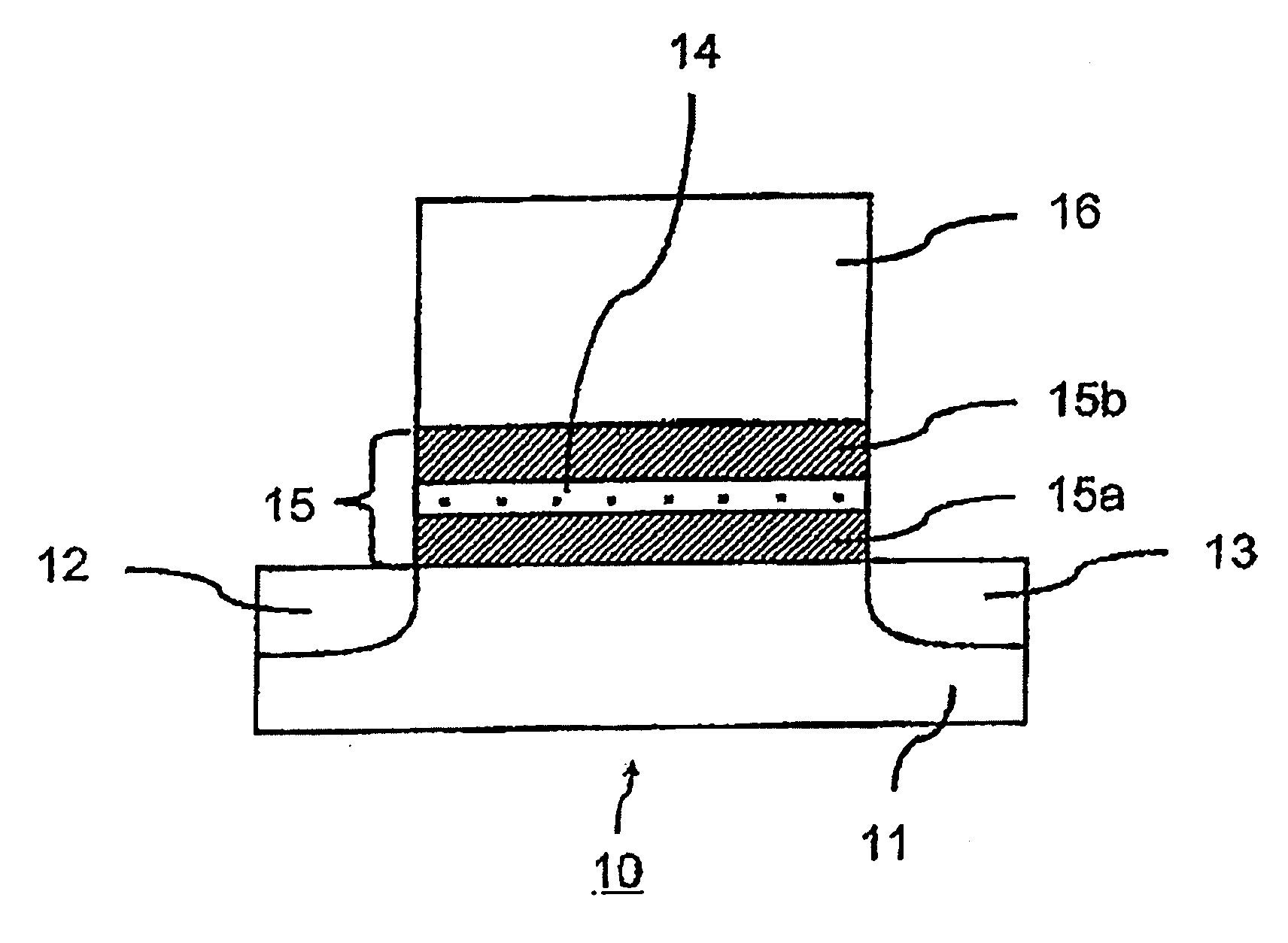
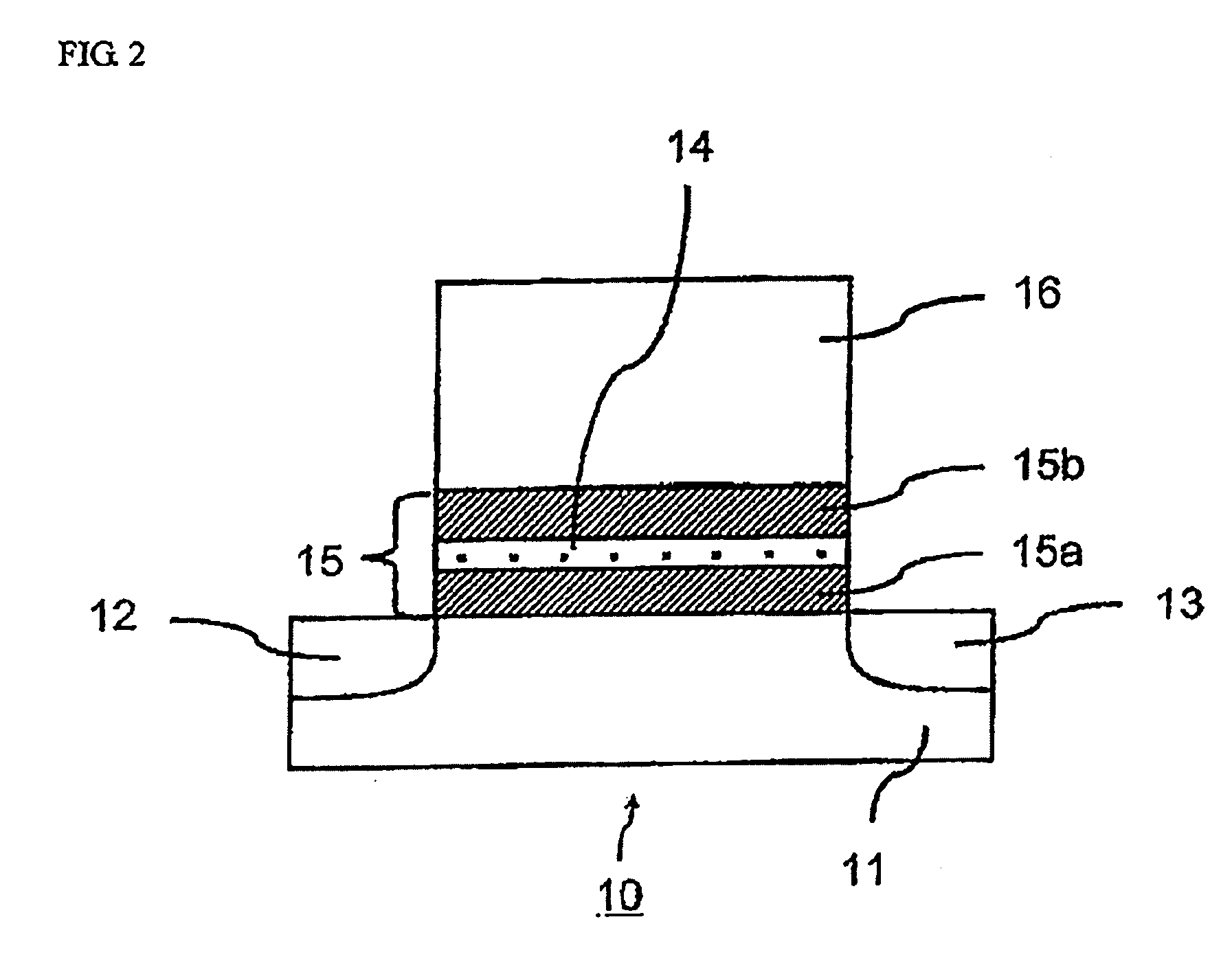
[0094]FIG. 4 is a cross-sectional view showing the method for producing the semiconductor memory device 10 according to the first embodiment of the present invention. As shown in FIG. 4(G), the semiconductor memory device 10 comprises: a semiconductor substrate 11; a first and a second impurities diffusion layers 12 and 13 disposed in the semiconductor substrate 11; a gate insulating film 15 disposed on the semiconductor substrate 11, and having a silicon oxide film 14 sandwiched between parts of the gate insulating film 15a and 15b, the silicon oxide film 14 tending to combine with the oxygen in the silicon oxide film and containing impurities discrete at an atomic level; and a first gate electrode 16 disposed on the semiconductor substrate 11 by way of the gate insulating film 15. Meanwhile, when using the parts of the gate insulating film 15a and15b that dispose the gate insulating film 15 other than the silicon oxide film 14, not being limited to silicon oxide film, that contain...

second embodiment

[0102]FIG. 7 is a cross-sectional view showing the method for producing the semiconductor memory device 10 according to the second embodiment of the present invention. As shown in FIG. 7(G), the semiconductor memory device 20 comprises: a semiconductor substrate 21; a first and second impurities diffusion layers 22 and 23 disposed in the semiconductor substrate 21; a gate insulating film 25 disposed on the semiconductor substrate 21, the gate insulating film 25 including a two-layer structure that comprises: a silicon oxide film 24 that contains the first impurities which tend to combine with oxygen in a silicon oxide film disposed on the semiconductor substrate 21 and which are discrete at an atomic level; and a second silicon oxide film 28 disposed thereon that contains the second impurities different from the first impurities, the two-layer structure being sandwiched between a part of the gate insulating film 25a and a part of the gate insulating film 25b; and a first gate electr...

third embodiment

[0110]FIG. 8 is a structure cross-sectional view showing the semiconductor memory device 30 according to the third embodiment of the present invention. Meanwhile, in the present embodiment, the silicon oxide film 34 that contains impurities which tend to combine with oxygen in the silicon oxide film and which are discrete at an atomic level is described only in the form of a silicon oxide film wherein the entire gate insulating film is disposed of a silicon oxide film; however, the other aspects of the gate insulating film structure is also acceptable. The same applies to the following embodiments. As shown in FIG. 8, the semiconductor memory device 30 comprises: a semiconductor substrate 31; a first impurities diffusion layer 32 and a second impurities diffusion layer 33 disposed in the semiconductor substrate 31; a gate insulating film disposed on the semiconductor substrate 31, and a first gate electrode 36 disposed on the semiconductor substrate 31 by way of the gate insulating ...


PUM


Abstract

Provided is a semiconductor memory device that can retain information by trapping electric charges into a trap level in a gate insulating film. The information retention capacity is improved by restricting lateral diffusion of electric charges. The semiconductor memory device is provided with a semiconductor substrate (11), first and second impurities diffusion layers (12; 13) disposed in the semiconductor substrate, a gate insulating film (15) disposed on the semiconductor substrate, and a first gate electrode (16) disposed on the semiconductor substrate by way of the gate insulating film (15). The gate insulating film (15) has a silicon oxide film (14) that contains impurities which tend to combine with oxygen in the silicon oxide film and which are discrete at an atomic level.

Description

TECHNICAL FIELD OF THE INVENTION[0001]The present invention is directed to a semiconductor memory device and a semiconductor device, and more particularly to a semiconductor memory device that can retain information by trapping charges into a trap level in a gate insulating film, and to a semiconductor device in which the semiconductor memory device is mounted.DESCRIPTION OF THE RELATED ART[0002]In order to sufficiently provide the current information relating to the present invention, any available references such as patent publications, laid-open patent applications and scientific literatures cited or identified in the present application are hereby incorporated by reference in their entirety.[0003]Recently, the demand for a non-volatile memory has increased as a rewritable semiconductor memory device. With regard to a flash memory which is a typical example of a non-volatile memory, a flash memory that employs a floating gate is in the mainstream. However, a thinner layer of the ...

Claims


Application Information

Patent Timeline
Patent Type & Authority Applications(United States)
IPC IPC(8): H01L29/792H01L29/78
CPCB82Y10/00H01L21/28273H01L21/28282H01L29/7923H01L29/42332H01L29/7887H01L29/42328H01L29/40114H01L29/40117
Inventor SUNAMURA, HIROSHI
Owner RENESAS ELECTRONICS CORP
Why Eureka
Try Eureka