Method of fabricating semiconductor components through implantation and diffusion in a semiconductor substrate

a technology of semiconductor components and substrates, applied in semiconductor devices, electrical equipment, transistors, etc., can solve the problems of reducing generating defects along the edge or boundary of the isolation trench, etc., to reduce the breakdown voltage of the device, prevent overflowing critical leakage current rates, and high thermal loading

Active Publication Date: 2005-05-05
ATMEL CORP +1
View PDF11 Cites 6 Cited by
  • Summary
  • Abstract
  • Description
  • Claims
  • Application Information

AI Technical Summary

Benefits of technology

[0014] This advantage of the invention must be understood further in connection with a balancing of another and somewhat-contrary advantage, as follows. For purposes of this comparative discussion, one could consider carrying out the diffusion of the well doping entirely after the formation of trenches, in order to thereby avoid or prevent the above-mentioned problem of out-diffusion in the outer edges or boundary areas of the respective well. On the other hand, however, if the deep trenches are etched before carrying out the high temperature drive step for diffusing the dopants into the wells, this would fundamentally give rise to the problem that defects can be generated along the edge or boundary of the isolation trench due to the high thermal loading that arises during the subsequent thermal drive step for achieving the entire dopant diffusion. In the subsequent operation of the semiconductor device, such defects can lead to undesirable leakage currents, which in turn undesirably reduce the breakdown voltage of the device.
[0015] Thus, in view of the above mentioned competing or contrary considerations, the inventive method aims to provide an acceptable or even optimized compromise between a substantial reduction or avoidance of the out-diffusion of opposite dopants in the outer edges or boundary areas of neighboring wells on the one hand, and an avoidance of defects to prevent exceeding critical leakage current rates in the later operation of the fabricated device on the other hand. In this regard, the first requirement arises from the urge to achieve a further size reduction of the device structure, while the second requirement arises from the demand to achieve a high breakdown resistance. These two opposite requirements are achieved in an optimized balanced manner through the inventive division of the high temperature thermal drive steps for carrying out the diffusion of the well doping into two separate high temperature diffusion drive steps that are separated in time from one another, namely at least one such step before and at least one such step after the formation of trench structures. Thereby, the problem of out-diffusion is reduced or avoided, while still reducing the temperature loading of the structure after the formation of trenches.
[0016] In a preferred embodiment of the invention, at least one (or some) of the trench structures is a deep trench that mutually electrically isolates component boxes (also called pockets or tubs) formed within the semiconductor substrate. In this manner, the lateral diffusion of well dopants through the trench structures is limited. Thereby, small well regions with high dopant concentrations and / or dopant concentrations that penetrate deeply into a volume of the semiconductor substrate can be produced, without giving rise to an undesired lateral out-diffusion problem along the edges or lateral boundaries of the wells. More particularly, such an undesired lateral diffusion is prevented by the interposed trenches.
[0017] It is further preferred that the deep trenches extend all the way down to an insulating layer on which the semiconductor substrate is disposed. Thereby, the neighboring wells are not only separated and isolated from one another in a defined manner at the surface of the semiconductor substrate, but also deeply within the volume of the semiconductor substrate.
[0018] According to another preferred embodiment of the invention, at least one (or some) of the trench structures is a shallow trench that at least partially bounds and serves to define a drift zone of a DMOS-transistor. In comparison to a typical Metal Oxide Semiconductor (MOS) transistor, a DMOS-transistor is distinguished in that it additionally has a drift zone, i.e. a zone in which the motion of the charge carriers is caused or effected only by an electrical field prevailing between the opposite ends of this zone. This drift zone is provided between an edge of a control gate and a drain region of the transistor. The lateral size or extension of the drift zone can be reduced by forming the drift zone along the boundaries (i.e. especially the sidewalls) of a shallow trench.
[0019] A further preferred feature of the invention is that the shallow trench is formed through a Shallow Trench Isolation (STI) process. In the STI technology, a shallow trench is formed by an anisotropic etching process between active regions covered with a nitride protective layer, and then the etched trench is filled with an insulating material such as silicon dioxide or polysilicon. Using the STI technology, for example, higher packing densities can be achieved in comparison to the use of a V-trench etching with a LOCOS (LOCal Oxidation of Silicon) mask.

Problems solved by technology

On the other hand, however, if the deep trenches are etched before carrying out the high temperature drive step for diffusing the dopants into the wells, this would fundamentally give rise to the problem that defects can be generated along the edge or boundary of the isolation trench due to the high thermal loading that arises during the subsequent thermal drive step for achieving the entire dopant diffusion.
In the subsequent operation of the semiconductor device, such defects can lead to undesirable leakage currents, which in turn undesirably reduce the breakdown voltage of the device.

Method used


Image

  • Method of fabricating semiconductor components through implantation and diffusion in a semiconductor substrate
  • Method of fabricating semiconductor components through implantation and diffusion in a semiconductor substrate
  • Method of fabricating semiconductor components through implantation and diffusion in a semiconductor substrate

Examples


Embodiment Construction

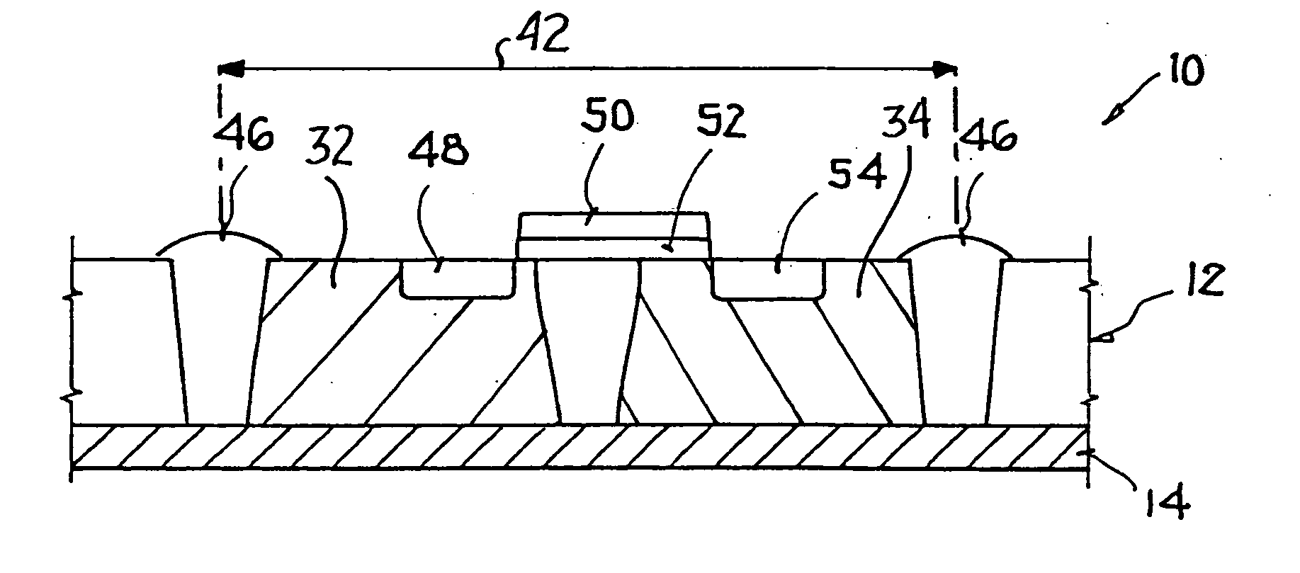
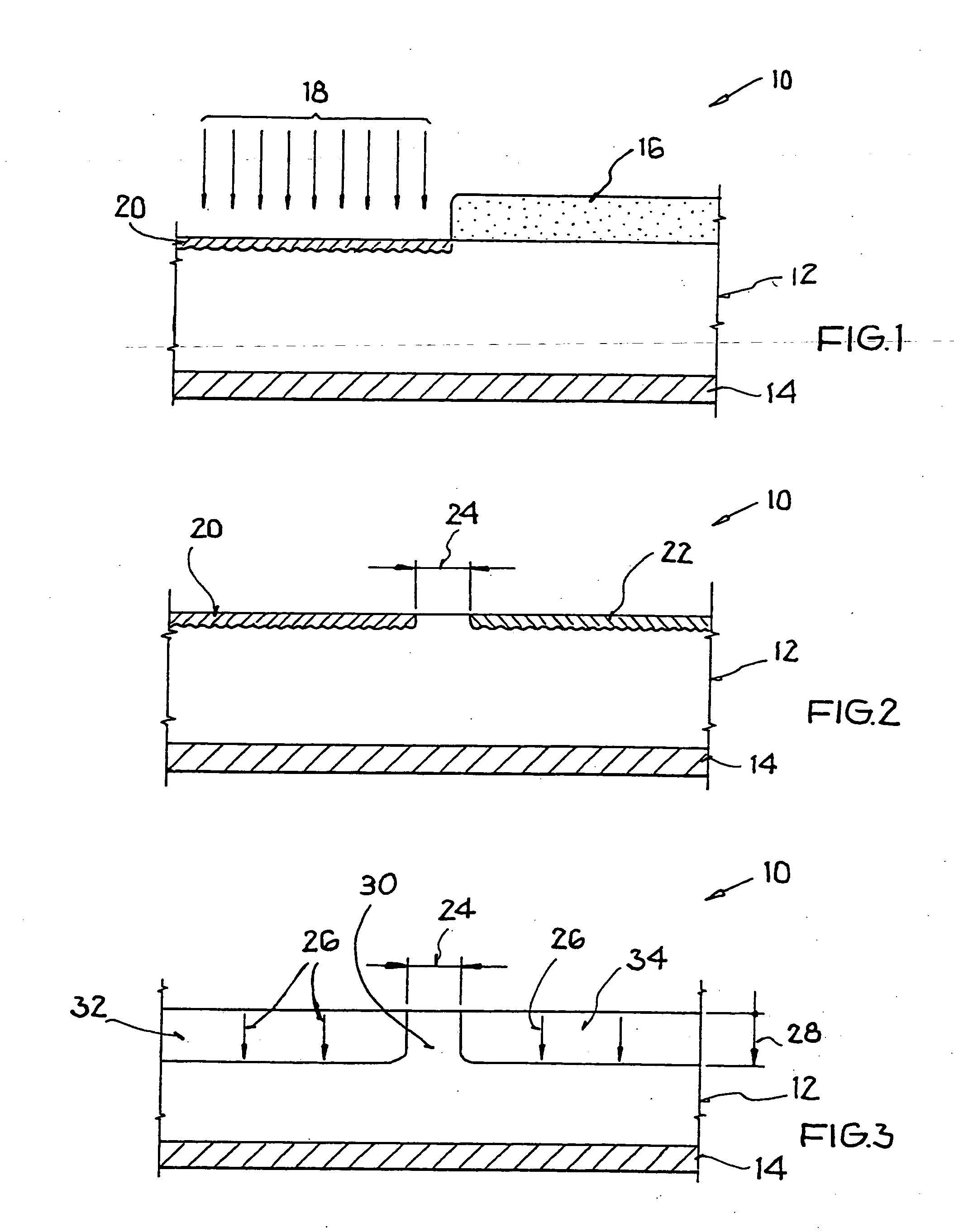
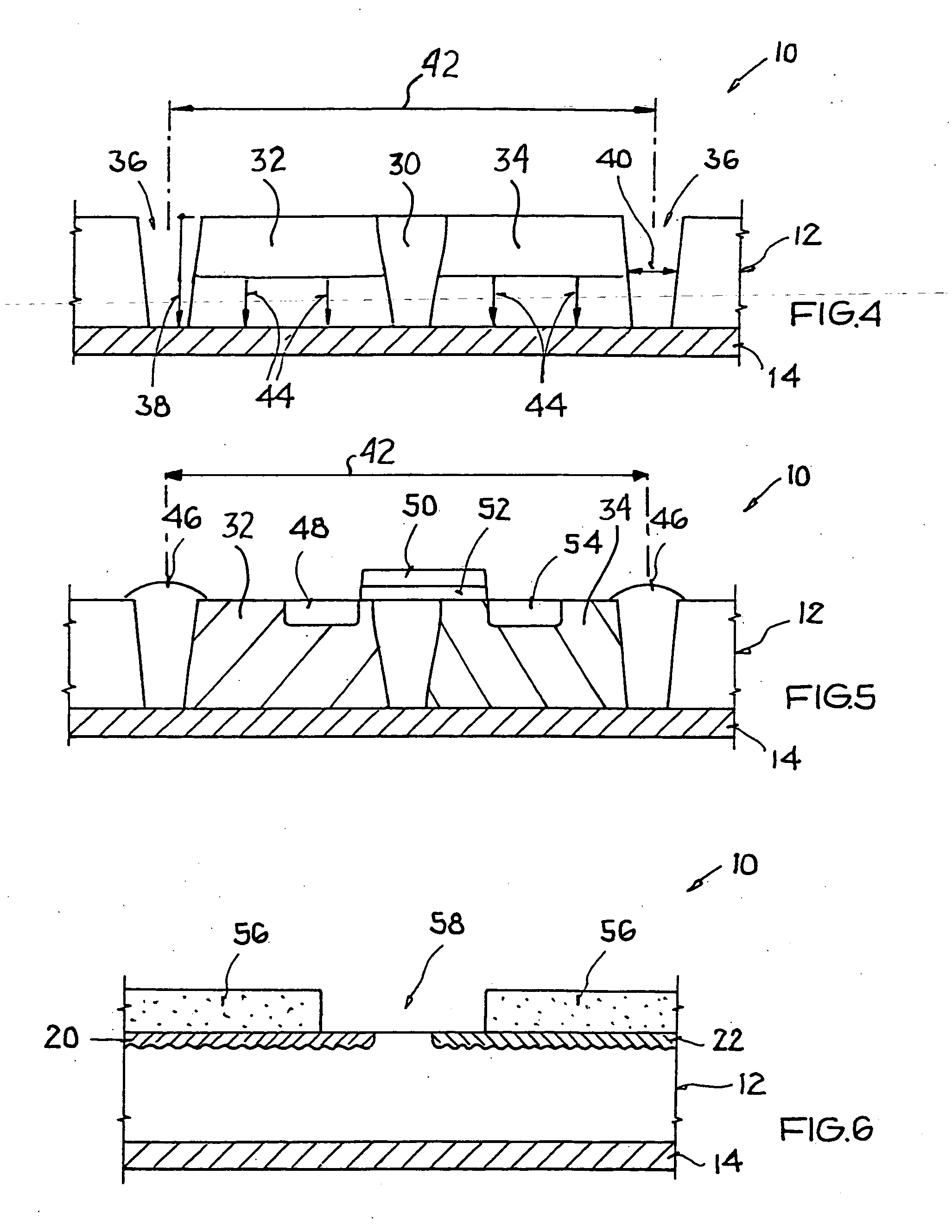
[0034]FIG. 1 schematically shows a cross-section of a portion of a semiconductor body 10 comprising a semiconductor substrate 12 on an insulating intermediate layer or isolating layer 14. A typical example of such a semiconductor body 10 is represented by a “Silicon On Insulator” (SOI) wafer. In this regard, the insulating intermediate layer 14 is typically realized as a silicon dioxide layer.

[0035] As a first step in a device or component fabrication process, respective well regions with different conductivity type will be formed in the semiconductor body 10. Namely, for forming these well regions with respective different conductivity of the respective majority charge carriers, different partial regions of the semiconductor substrate 12 will respectively be doped with dopants of different valence, so that the different conductivity types result in the respective well regions. To achieve a P-type conductivity in a four-valent semiconductor substrate material such as silicon, for e...


PUM


Abstract

A semiconductor element such as a DMOS-transistor is fabricated in a semiconductor substrate. Wells of opposite conductivity are formed by implanting and then thermally diffusing respective well dopants into preferably spaced-apart areas in the substrate. At least one trench and active regions are formed in the substrate. The trench may be a shallow drift zone trench of a DMOS-transistor, and/or a deep isolation trench. The thermal diffusion of the well dopants includes at least one first diffusion step during a first high temperature drive before forming the trench, and at least one second diffusion step during a second high temperature drive after forming the trench. Dividing the thermal diffusion steps before and after the trench formation achieves an advantageous balance between reducing or avoiding lateral overlapping diffusion of neighboring wells and reducing or avoiding thermally induced defects along the trench boundaries.

Description

PRIORITY CLAIM [0001] This application is based on and claims the priority under 35 U.S.C. §119 of German Patent Application 103 45 345.8, filed on Sep. 19, 2003, the entire disclosure of which is incorporated herein by reference. FIELD OF THE INVENTION [0002] The invention relates to a method for fabricating semiconductor components in a semiconductor substrate by forming wells with different conductivity types and forming trench structures in the substrate. BACKGROUND INFORMATION [0003] A well is a three-dimensional region or portion of a semiconductor substrate, having majority charge carriers of a different conductivity type (for example P-type) in comparison to the majority charge carriers of the surrounding portion of the substrate around the well (for example N-type). As a result, blocking or non-conductive PN-junctions will be formed along the peripheral edges or boundaries of the well, in connection with a suitable electrical reverse-biasing thereof, whereby these PN-juncti...

Claims


Application Information

Patent Timeline
Patent Type & Authority Applications(United States)
IPC IPC(8): H01L21/225H01L21/265H01L21/336H01L21/76H01L21/762H01L21/8238H01L27/08H01L29/10H01L29/78H01L29/786
CPCH01L21/2253H01L21/26586H01L21/76237H01L21/76283H01L29/7835H01L21/823892H01L29/1045H01L29/66659H01L21/823878
Inventor DIETZ, FRANZDUDEK, VOLKERGRAF, MICHAEL
Owner ATMEL CORP
Why Eureka
Try Eureka