Charged balanced devices with shielded gate trench

a balanced device and gate trench technology, applied in the direction of semiconductor devices, basic electric elements, electrical apparatus, etc., can solve the problems of less desirable floating islands and slow electrical transitions, and achieve the effects of reducing channel performance sensitivity, slow electrical transitions, and good control of transistor cell performan

Active Publication Date: 2010-02-25
ALPHA & OMEGA SEMICON INC
View PDF2 Cites 41 Cited by
  • Summary
  • Abstract
  • Description
  • Claims
  • Application Information

AI Technical Summary

Benefits of technology

[0015]It is therefore an aspect of the present invention to provide a new and improved device structure and manufacturing method to form the doped columns in the drift regions for charge balance with simple and convenient processing steps. There are no etch-backs or CMP (chemical mechanical polishing) required thus reducing the processing steps and can be implemented with just forming a single thin epitaxial layer, simultaneously grown in and over deep trenches and on the top surface on the areas surrounding the deep trenches to achieve the super junction structure. The portion of the epitaxial layer in the trenches forms the epitaxial columns. The portion of the epitaxial layer grown over the deep trenches and over the top surface on the areas surrounding the deep trenches form the thin top epitaxial layer, in which trench MOSFET cells are formed. Both portions of the epitaxial layer may be grown at the same time as a single epitaxial layer. The trench gates of the transistor cells are further shielded with doped shielding regions implanted through the trench gates into the drift region below the gate thus forming self-aligned dopant shielding regions to shield the sensitive gates during the voltage breakdown therefore the above discussed difficulties and limitations are resolved. The doped shielding regions reduce the peak electric field at the trench gates; they also reduce the impact ionization rate and increase the breakdown voltage. The resulting structure has improved reliability and stability of electrical parameters. The doped shielding regions are formed under the accumulation region below the trench gates, and do not need to contact the trench gates. An additional dopant layer below the gate trench having the same conductivity type as the accumulation region can ensure that the doped shielding region does not contact the gate trench, which may allow more current to pass through when the device is switched on.
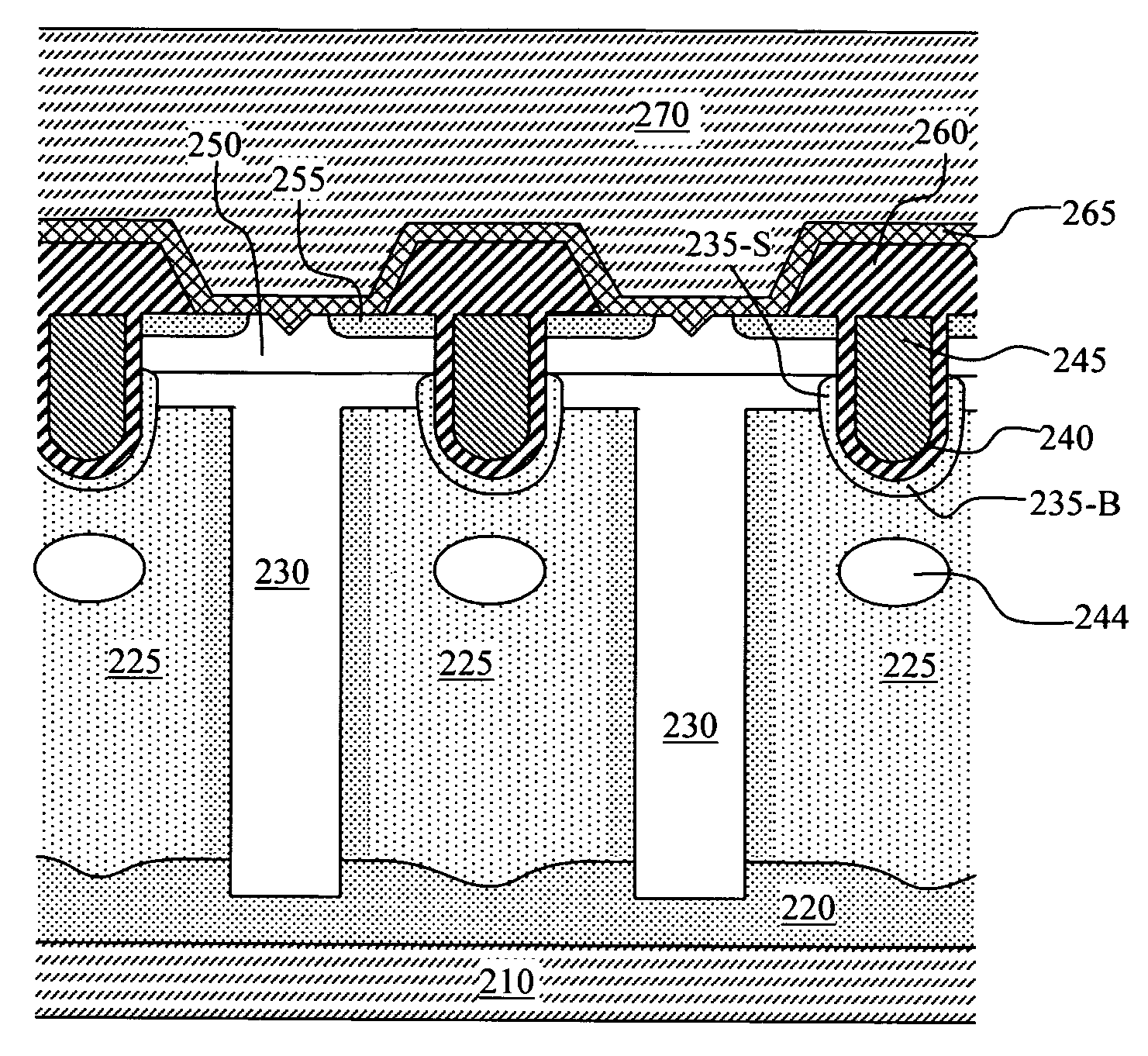
[0017]Specifically, it is an aspect of the present invention to provide a new and improved device structure and manufacturing method to form the epitaxial layer in deep trenches with a thin top epitaxial layer portion covering over the top surface of the device. A portion of this epitaxial layer also serves as the body region of the MOSFET (p-type in the case of n-channel MOSFET). Furthermore, the MOSFET cells are formed in this top thin epitaxial layer as trench MOSFET. Trench gates are opened through the top thin epitaxial layer with optional trench sidewalls and trench bottom dopant implant zones to eliminate the sensitivity of the channel performance that may be affected by the depth of the trench gates and the dopant concentration of the epitaxial layer. A plurality of doped shielding regions are also implanted through the gate trenches into the drift region beneath the gates before the gate trenches are filled with a gate polysilicon layer. The doped shielding regions are of the same conductivity type as the body region of the MOSFET and function as gate shielding dopant regions which are self-aligned with the gate trenches. The doped shielding regions may be floating islands, or they may be tied (biased) to the epitaxial layer in the deep trenches and thus tied to the body region. Typically, floating islands are less desirable because they trap charges and make the device drift; the trapped charges also slow electrical transitions since the trapped charges take time to diffuse out. The performance of the transistor cells can be well controlled and adjusted by simplified and convenient processing steps. The super-junction configurations disclosed in this invention is further scalable for broad ranges of applications.
[0018]It is another aspect of the present invention to provide a new and improved device structure and manufacturing method to form the power transistor cells on a thin top layer formed as an epitaxial layer covering over the deep trenches and over the top surface surrounding and above the deep trenches. Ion implantation (having an opposite conductivity type as the epitaxial layer filling the deep trenches) through the deep trench sidewalls may adjust the dopant concentration of the drift regions surrounding the deep trenches to adjust and control the device performance parameters including the charge balance, Rdson and breakdown voltage. The ion implantation thus provides charge control to further adjust and fine tune the performance of the semiconductor power devices for different types of applications.
[0020]It is another aspect of the present invention to provide new and improved device structure and manufacturing method to form the power transistor cells with deeper trench gates in a thin top layer formed as an epitaxial layer covering over epitaxial columns and on the top surface surrounding areas above the epitaxial columns. The trench gates penetrate through the top thin epitaxial layer and extend into the substrate regions thus a trench bottom dopant implant for connecting to the accumulation region may no longer be necessary. The trench gates are still shielded by the gate-shielding dopant regions implanted through the bottom surfaces of the gate trenches to form aligned dopant regions for shielding the sensitive trench gates during a voltage breakdown. A trench bottom dopant implant may still be used to ensure that the gate-shielding dopant regions do not contact the gate trenches.

Problems solved by technology

Typically, floating islands are less desirable because they trap charges and make the device drift; the trapped charges also slow electrical transitions since the trapped charges take time to diffuse out.

Method used


Image

  • Charged balanced devices with shielded gate trench
  • Charged balanced devices with shielded gate trench
  • Charged balanced devices with shielded gate trench

Examples


Embodiment Construction

[0030]Referring to FIG. 2 for a cross sectional view of a MOSFET device 100 that illustrates the new concepts including the new structural and manufacturing features of this invention. The details of the MOSFET device 100 will be further described and explained in FIG. 3 below. The MOSFET device 100 is supported on a substrate 105 that includes an N+ doped bottom region 120 functioning as drain contact region doped through deep trenches 130 (after back-grinding, as shown in FIG. 3 below) that is filled with an epitaxial layer therein. The substrate 105 may include a top portion 125 in which the deep trenches 130 are formed. For the example of an n-channel MOSFET, the substrate 105 is n-type, and the epitaxial layer in the deep trenches 130 is p-type. The MOSFET transistor cells are supported on the single thin epitaxial layer filling in epitaxial column trenches 130 and covering over the top surface surrounding the P-epitaxial columns that has the P-epitaxial filling in the column t...


PUM


Abstract

This invention discloses a semiconductor power device disposed on a semiconductor substrate includes a plurality of deep trenches with an epitaxial layer filling said deep trenches and a simultaneously grown top epitaxial layer covering areas above a top surface of said deep trenches over the semiconductor substrate. A plurality of trench MOSFET cells disposed in said top epitaxial layer with the top epitaxial layer functioning as the body region and the semiconductor substrate acting as the drain region whereby a super-junction effect is achieved through charge balance between the epitaxial layer in the deep trenches and regions in the semiconductor substrate laterally adjacent to the deep trenches. Each of the trench MOSFET cells further includes a trench gate and a gate-shielding dopant region disposed below and substantially aligned with each of the trench gates for each of the trench MOSFET cells for shielding the trench gate during a voltage breakdown.

Description

[0001]This Patent Application is a Continuation in Part (CIP) Application of a co-pending Application with a Ser. No. 12 / 229,250 filed by a common Inventor of this Application on Aug. 20, 2008. The disclosure made in that Application is hereby incorporated by reference.BACKGROUND OF THE INVENTION[0002]1. Field of the Invention[0003]The invention relates generally to vertical semiconductor power devices. More particularly, this invention relates to configurations and methods implemented with a single thin epitaxial layer with improved manufacturability for manufacturing flexibly scalable charge balanced vertical semiconductor power devices with a super-junction structure and shielded gate trench with simple manufacturing processes flexibly adjustable for applications to different targeted breakdown voltages.[0004]2. Description of the Prior Art[0005]Conventional manufacturing technologies and device configuration to further increase the breakdown voltage with reduced series resistanc...

Claims


Application Information

Patent Timeline
Patent Type & Authority Applications(United States)
IPC IPC(8): H01L29/78H01L21/336
CPCH01L21/26586H01L29/0623H01L29/0634H01L29/0696H01L29/0873H01L29/7813H01L29/1095H01L29/41766H01L29/4236H01L29/4238H01L29/66734H01L29/0878
Inventor HEBERT, FRANCOIS
Owner ALPHA & OMEGA SEMICON INC
Why Eureka
Try Eureka