Method of manufacturing semiconductor device, and semiconductor device

a manufacturing method and technology of semiconductor devices, applied in the direction of coatings, transistors, basic electric elements, etc., can solve the problems of cu-plated film lowering and electromigration resistance, and achieve the effects of preventing copper diffusion, suppressing copper diffusion, and reducing cu-plated film lowering

Active Publication Date: 2010-02-25
RENESAS ELECTRONICS CORP
View PDF14 Cites 41 Cited by
  • Summary
  • Abstract
  • Description
  • Claims
  • Application Information

AI Technical Summary

Benefits of technology

[0016]According to the above embodiment, the oxide layer containing the first metal element can more suppress the diffusion of copper and holes at the upper face of the copper alloy wiring, as compared with metal diffusion-preventing films (SiCN, SiN) that are generally adopted for the purpose of preventing the diffusion of copper. That is, by forming the oxide layer, it is possible to retard the diffusion of copper and holes at the upper face of copper alloy wiring. Accordingly, as a result, such faults as electromigration and stress migration of copper alloy wiring can be suppressed.

Problems solved by technology

Consequently, there is such a problem that the concentration of the additive metal element in the Cu-plated film lowers to lower the electromigration resistance.

Method used


Image

  • Method of manufacturing semiconductor device, and semiconductor device
  • Method of manufacturing semiconductor device, and semiconductor device
  • Method of manufacturing semiconductor device, and semiconductor device

Examples


embodiment 1

[0033]Hereinafter, a method of manufacturing a semiconductor device according to an embodiment 1 will be described on the basis of process cross-sectional views.

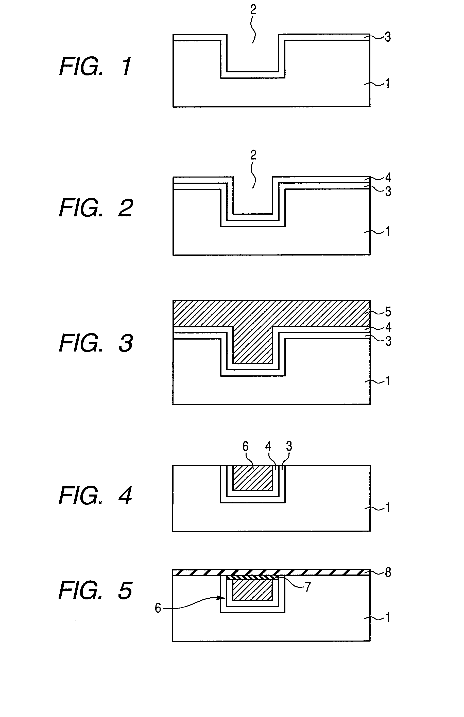
[0034]Firstly, as shown in FIG. 1, over a semiconductor substrate (not shown) in which electronic parts including a transistor have been formed, a first interlayer insulating film (that may be comprehended as a first interlayer film) 1 is formed. Then, within the surface of the first interlayer insulating film 1, a groove 2 having a prescribed shape for lower layer wiring is formed (refer to FIG. 1) by a general photolithographic technology.

[0035]Further, for the upper face of the first interlayer insulating film 1 and for the inside of the groove 2 for lower layer wiring, a film-forming treatment is provided by a sputtering treatment or a CVD (Chemical Vapor Deposition) method. This causes the formation of a first barrier metal 3 on the bottom and side faces of the groove 2 for lower layer wiring, and over the first interla...

embodiment 2

[0071]Hereinafter, on the basis of the process cross-sectional view, a method according to an embodiment 2 for manufacturing a semiconductor device will be described.

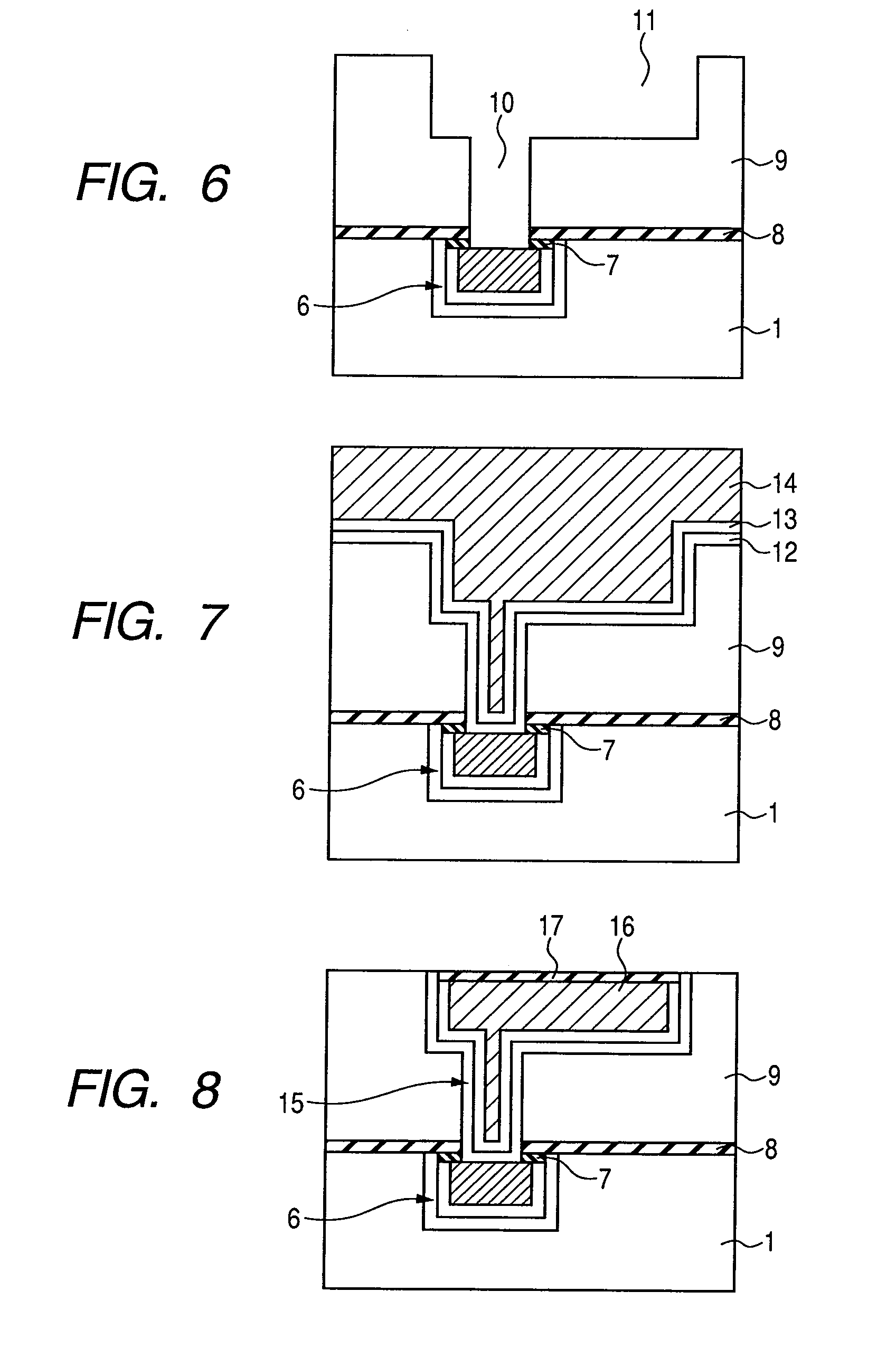
[0072]Firstly, the manufacturing processes described in the embodiment 1 using FIGS. 1 to 5 are performed also in the present embodiment in the same way. This results in the formation of the structure as shown in FIG. 5.

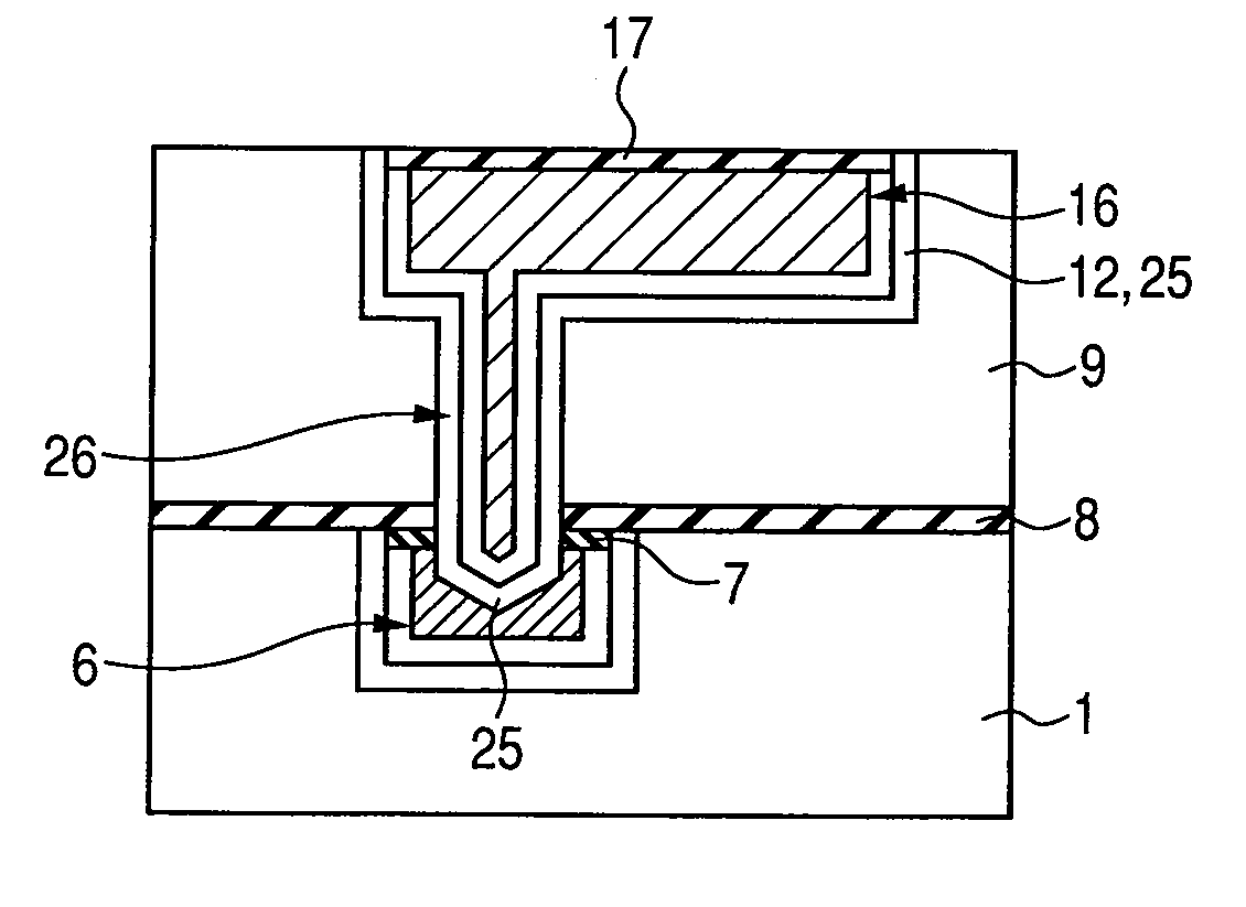
[0073]In the structure as shown in FIG. 5, the lower layer Cu alloy wiring 6 having a prescribed shape is formed in the plane of the first interlayer insulating film 1. Here, between the lower layer Cu alloy wiring 6 and the first interlayer insulating film 1, the first barrier metal 3 is formed. Also, over the whole upper face of the lower layer Cu alloy wiring 6, the oxide layer 7 being the oxide of the first metal element is formed. Above the upper face of the lower layer Cu alloy wiring 6 (more specifically, above the oxide layer 7) and on the upper face of the first interlayer insulating film 1, the...


PUM

PropertyMeasurementUnit
temperatureaaaaaaaaaa
pressureaaaaaaaaaa

Abstract

The present invention aims at providing a method of manufacturing a semiconductor device capable of suppressing metal diffusion from the upper face of wiring.
In the present invention, a copper seed film containing copper and a first metal element is formed in a groove formed in a first interlayer film over a semiconductor substrate. After that, a copper plating treatment is performed. After that, a first heat treatment is performed in a first atmosphere in which the copper layer is not oxidized. Then, an excess metal layer of copper alloy is removed and copper alloy wiring is formed in the groove. After that, a second heat treatment is performed in a second atmosphere containing oxygen to form an oxide layer being the oxide of the first metal element over the surface of the copper alloy wiring.

Description

CROSS REFERENCE TO RELATED APPLICATIONS[0001]The disclosure of Japanese Patent Application No. 2008-213563 filed on Aug. 22, 2008 including the specification, drawings and abstract is incorporated herein by reference in its entirety.BACKGROUND OF THE INVENTION[0002]The present invention relates to a method of manufacturing a semiconductor device and to a semiconductor device, and, in particular, to a method of manufacturing a semiconductor device and to a semiconductor device, the semiconductor device having wiring and a via plug containing copper as a component.[0003]For wiring layers of semiconductor devices in recent years, Cu (copper) damascene wirings having high reliability and high performance have been frequently used. Hereinafter, the conventional manufacturing procedure of Cu damascene wiring in semiconductor devices will be described.[0004]Firstly, over a semiconductor substrate in which electronic parts including transistors have been formed, a first interlayer insulatin...

Claims


Application Information

Patent Timeline
Patent Type & Authority Applications(United States)
IPC IPC(8): H01L23/48H01L21/3205
CPCH01L21/2855H01L21/76805H01L21/76832H01L21/76834H01L21/76843H01L21/76864H01L21/76873H01L2924/0002H01L21/76883H01L21/76888H01L23/53233H01L23/53238H01L2924/00
Inventor MAEKAWA, KAZUYOSHIMORI, KENICHIOMORI, KAZUYUKIKOYAMA, YUKI
Owner RENESAS ELECTRONICS CORP
Why Eureka
Try Eureka