Detecting method, detecting apparatus, detection sample cell, and detecting kit

a detection method and sample cell technology, applied in the field of detection methods, detecting apparatuses, and detecting kits, can solve the problems of signal intensities fluctuation, bsub>1 /sub>to collapse along the surface, and achieve the effect of maximizing the effect of electric field enhancement, maximizing the degree of enhancement, and efficient utilization

Inactive Publication Date: 2010-02-25
FUJIFILM CORP
View PDF7 Cites 4 Cited by
  • Summary
  • Abstract
  • Description
  • Claims
  • Application Information

AI Technical Summary

Benefits of technology

[0062]In the detecting method and the detecting apparatus of the present invention, detection is performed in a state in which a first electric charge is imparted to the sensor portion, and a second electric charge opposite the first electric charge is imparted onto the fluorescent substance that functions as fluorescent labels. Accordingly, the fluorescent labels are drawn to the vicinity of the surface of the sensor portion, at which the electric field enhancing effect is great, due to static electric interactions. Therefore, amounts of light which are generated due to excitation of the fluorescent labels in a state that the fluorescent labels are in the vicinity of the surface of the sensor portion can be detected. As a result, the electric field at the surface of the sensor por...

Problems solved by technology

Therefore, differences occur in signals by slight changes in distance between the surfaces and fluorescent labels, resulting in a problem that signal fluctuations occur.
In addition, the primary antibodies B1 are not always immobilized onto the surface of the sensor portion in an upright state, and there...

Method used


Image

  • Detecting method, detecting apparatus, detection sample cell, and detecting kit
  • Detecting method, detecting apparatus, detection sample cell, and detecting kit
  • Detecting method, detecting apparatus, detection sample cell, and detecting kit

Examples


fourth embodiment

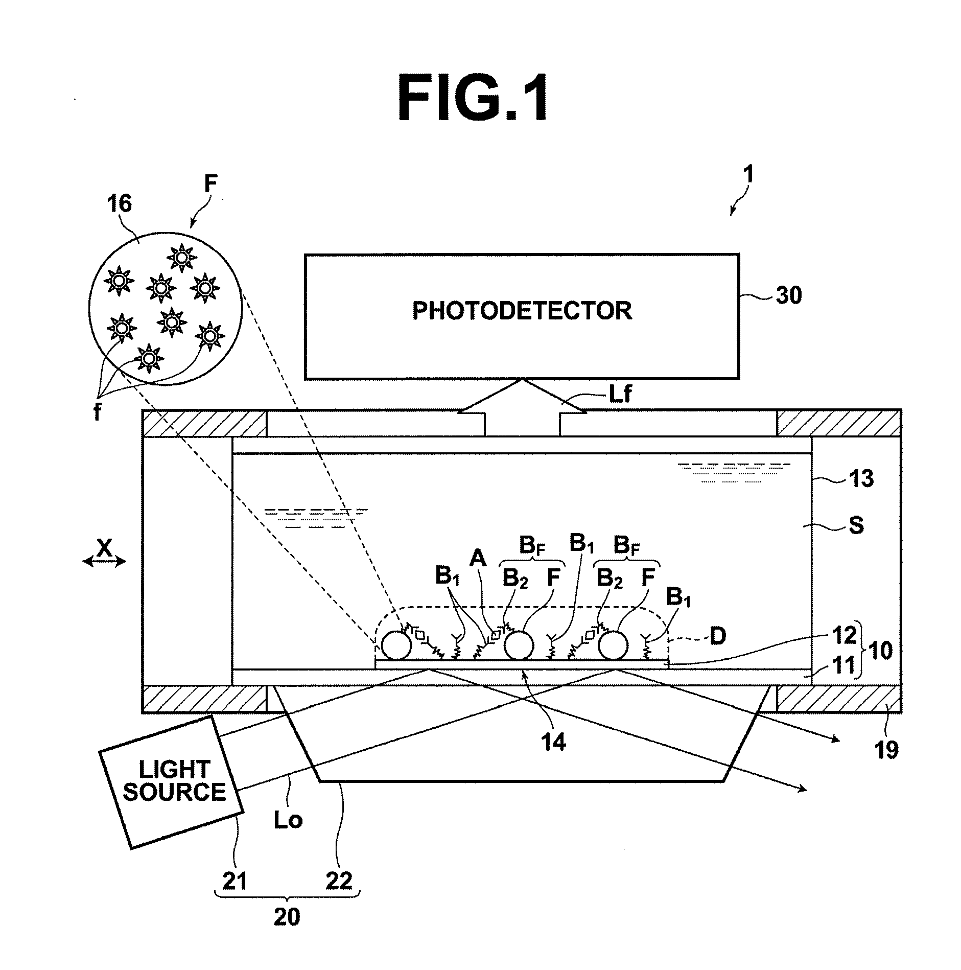
[0138]A detecting method and a detecting apparatus according to a fourth embodiment will be described with reference to FIG. 7. FIG. 7 is a schematic diagram that illustrates the entirety of the detecting apparatus 4 of the fourth embodiment. The detecting method and the detecting apparatus of the fourth embodiment employs a sensor chip equipped with an optical waveguide layer on a metal layer. An optical waveguide mode is excited at the optical waveguide layer, which generates an enhanced optical field. Fluorescence which is excited by the enhanced optical field is detected.

[0139]The construction of the detecting apparatus 4 illustrated in FIG. 7 is the same as the construction of the detecting apparatus of the first embodiment. However, the sensor chip which is employed is different, and the different sensor chip results in a different mechanism of electric field enhancement.

[0140]A sensor chip 10″ which is utilized in the fourth embodiment is equipped with a metal layer 12a and a...

fifth embodiment

[0145]A detecting method and a detecting apparatus according to a fifth embodiment will be described with reference to FIG. 8. FIG. 8 is a schematic diagram that illustrates the entirety of the detecting apparatus 5 of the fifth embodiment. The detecting method and the detecting apparatus of the fifth embodiment employs a sensor chip equipped with an optical waveguide layer on a metal layer. An optical waveguide mode is excited at the optical waveguide layer, which generates an enhanced optical field. Radiant light that radiates toward the side of a dielectric plate opposite the side on which a metal layer is formed, from surface plasmon which is newly excited at the metal layer by fluorescence generated by fluorescent labels due to excitation is detected.

[0146]The construction of the detecting apparatus 5 illustrated in FIG. 8 is the same as the construction of the detecting apparatus of the third embodiment. The sensor chip which is employed in the detecting method of the fifth em...

first embodiment

[0159]FIG. 10A is a plan view that illustrates the construction of a detection sample cell 50, and FIG. 10B is a cross sectional side view of the detection sample cell 50.

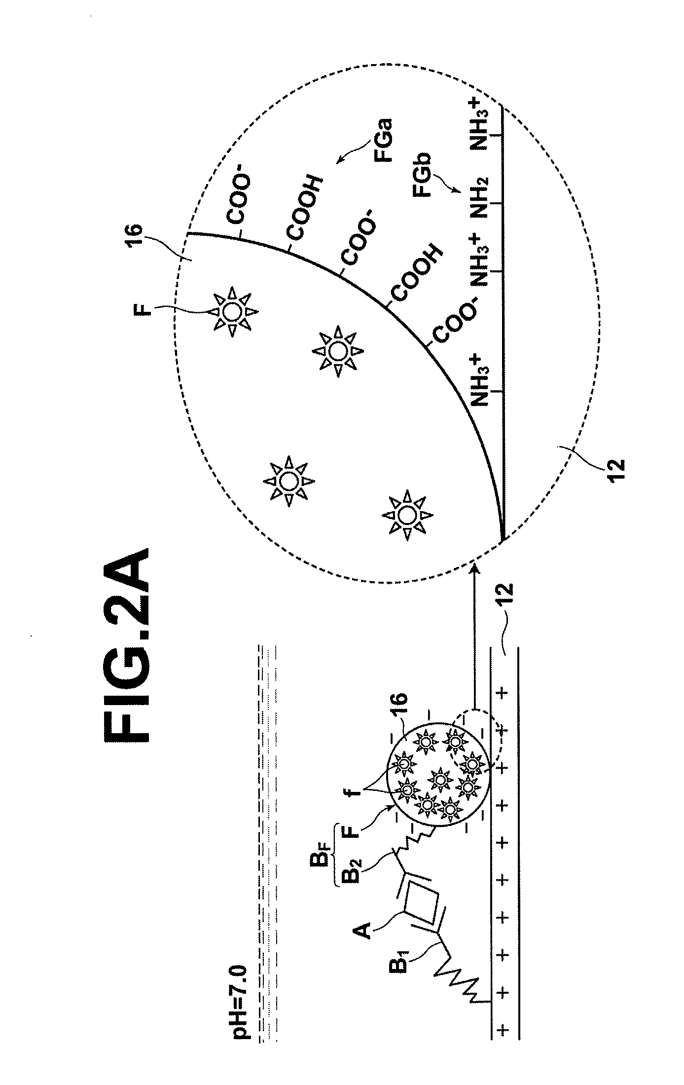
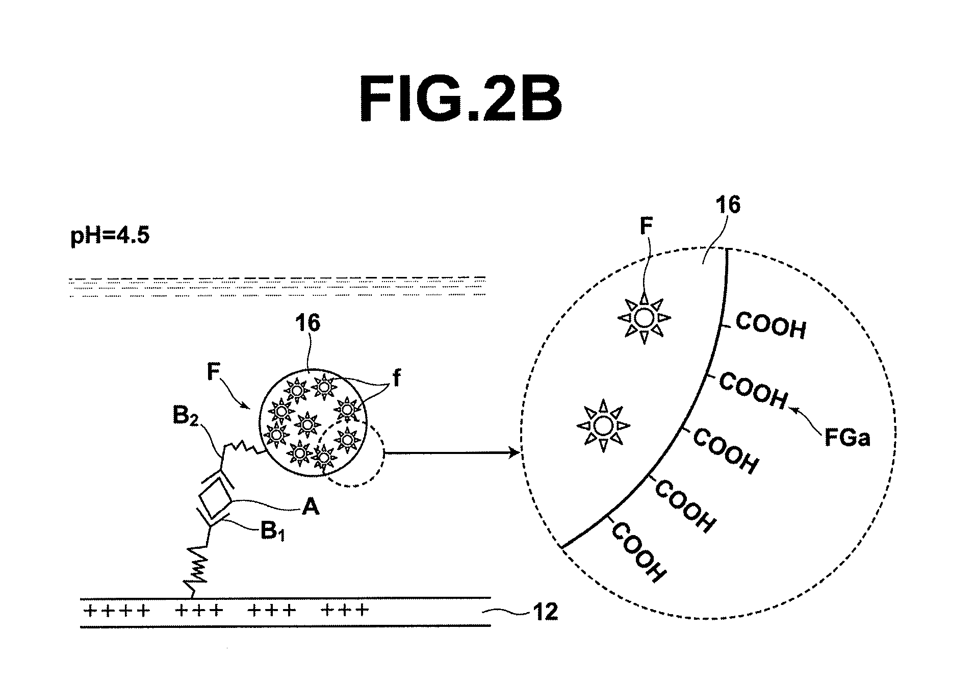
[0160]The detection sample cell 50 is equipped with: a base 51, which is formed by a dielectric plate; a spacer 53 for holding the liquid sample S on the base 51 and which forms a channel 52 for the liquid sample S; and an upper plate 54, which is a glass plate having an injection opening 54a through which the liquid sample S is injected, and an air aperture 54b through which the liquid sample S is expelled after flowing through the channel 52. Metal layers 58a and 59a are provided at predetermined regions of the base 51 between the injection opening 54a and the air aperture 54b, that is, at sample contacting surfaces of the base 51, to form sensor portions 58 and 59. Here, the sensor portions have first electrical charges imparted on the surfaces thereof. A membrane filter 55 is provided at a position between the ...


PUM


Abstract

A sample is supplied onto the sensor portion of a sensor chip. An excitation light beam is irradiated to generate an enhanced optical field to be generated on the sensor portion. Fluorescent labels are excited, and the amount of a detection target substance is detected, based on the amount of light which is generated due to excitation of the fluorescent labels. A first electric charge is present on the surface of the sensor portion. A fluorescent substance having fluorescent pigment molecules which are enveloped in a light transmitting material that transmits fluorescence generated by the fluorescent pigment molecules, the surfaces of which are charged with second electric charges opposite the first electric charge on the surface are employed as the fluorescent labels. The fluorescent substance is attracted to the sensor portion by static electric interactions between the two charges.

Description

BACKGROUND OF THE INVENTION[0001]1. Field of the Invention[0002]The present invention is related to a detecting method, for detecting detection target substances within samples, a detection sample cell and a detecting kit.[0003]2. Description of the Related Art[0004]Fluorometry is conventionally used in biological measurements and the like, as an easy and highly sensitive measuring method. In fluorometry, a sample, which is considered to contain a detection target substance that emits fluorescence when excited by light having a specific wavelength, is irradiated with an excitation light beam of the aforementioned specific wavelength. The presence of the detection target substance can be confirmed quantitatively by detecting the fluorescence due to the excitation. In the case that the detection target substance is not a fluorescent substance, the detection target sample is labeled with fluorescent labels, such as organic fluorescent pigment. Thereafter, fluorescence is detected in th...

Claims


Application Information

Patent Timeline
IPC IPC(8): G01N33/53C12M1/34
CPCG01N33/54373
Inventor OHTSUKA, HISASHI
Owner FUJIFILM CORP
Why Eureka
Try Eureka