Load sense and active noise reduction for I/O circuit

a load sense and active noise reduction technology, applied in logic circuits, voltage/current interference elimination, reliability increasing modifications, etc., can solve the problems of reduced system performance and signal transition speed obtained at the cost of high noise levels, and achieve low noise levels and high speed

Active Publication Date: 2010-03-04
NAT SEMICON CORP
View PDF6 Cites 9 Cited by
  • Summary
  • Abstract
  • Description
  • Claims
  • Application Information

AI Technical Summary

Benefits of technology

[0008]The present invention provides feedback control for a capacitive feedback I / O circuit of the type discussed above with respect to FIGS. 2A and 2B. Capacitive feedback control circuitry controls the time and point at which the feedback capacitor is applied to the gate drive of the I / O circuit output stage. Active device feedback control circuitry controls the output stage gate drive. The addition of these control features provides a high speed I / O circuit, but with very low noise levels.

Problems solved by technology

As shown in FIG. 1B, although this “worst case” design is relatively fast, the signal transition speed is obtained at the cost of high noise levels.
As shown in FIG. 2B, however, the effect of the transition capacitors 112, 114 is to lower the noise levels of the low-to-high and high-to-low transitions, but at the cost of slowing down the low-to-high transition threshold edge ViH and the high-to-low transition edge ViL required to drive the load, thereby resulting in reduced system performance.

Method used


Image

  • Load sense and active noise reduction for I/O circuit
  • Load sense and active noise reduction for I/O circuit
  • Load sense and active noise reduction for I/O circuit

Examples


Embodiment Construction

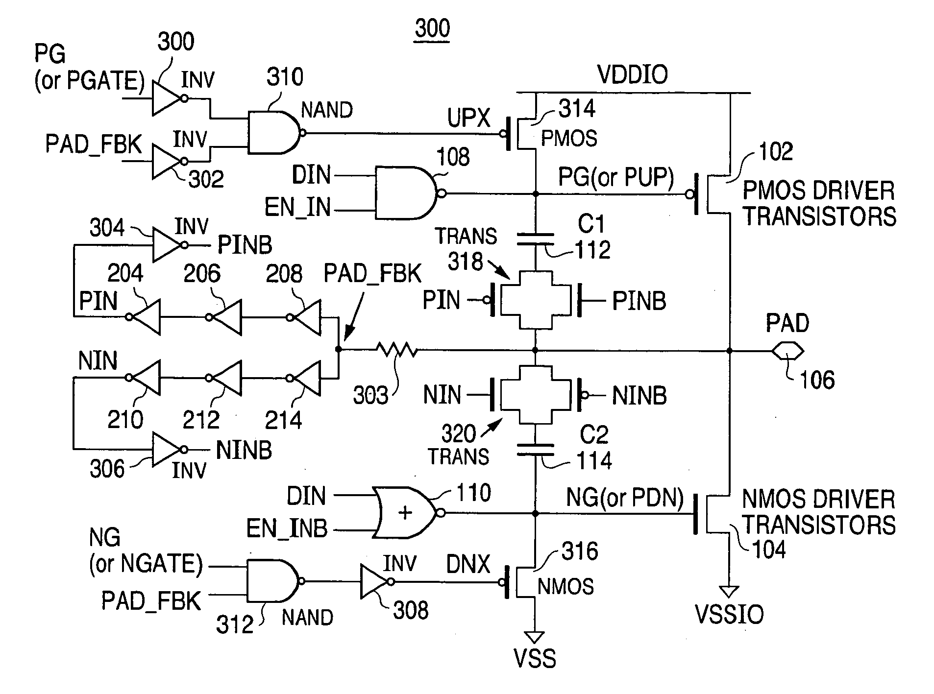
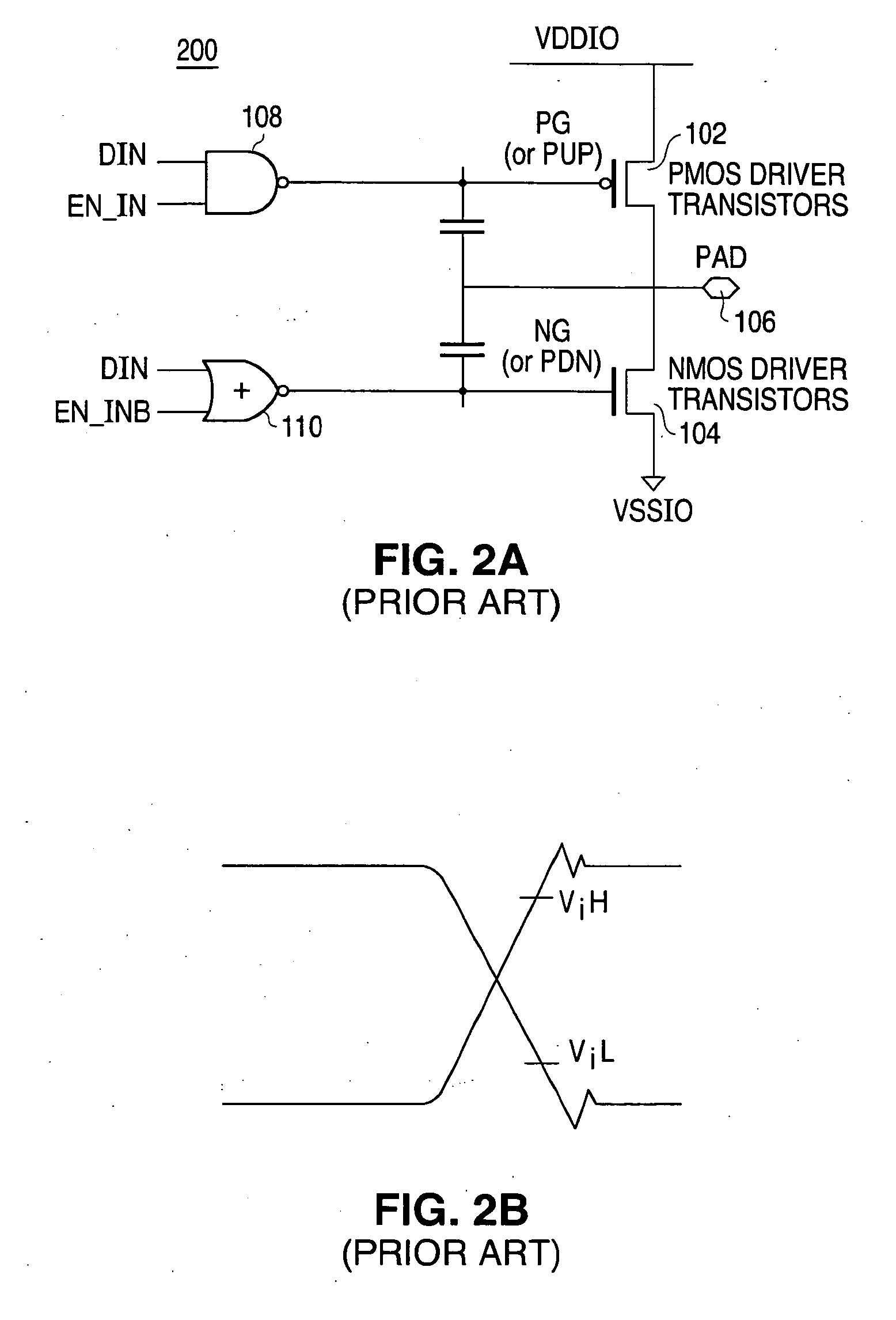
[0016]FIG. 3A shows an I / O circuit 300 in which a low voltage data signal from the core circuit has amplified and stabilized and the lower voltage VDD level signal from the core circuit is level-shifted to high voltage VDDIO level and sent to a pre-driver NAND 108 and a pre-driver NOR gate 110, which combine an enable control signal from another level-shifter to provide the logic functions for the PMOS driver transistor 102 and the NMOS driver transistor 104. FIG. 3A also shows the feedback capacitors 112, 114 of the FIG. 2A design.

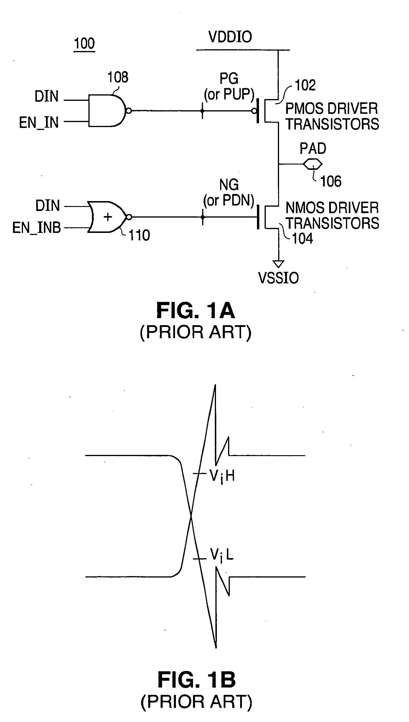
[0017]As discussed above during driver pull-up time, the pre-driver NAND gate 108 usually provides a high-to-low pulse to turn on the gate of PMOS driver transistor 102 to allow the power supply VDDIO to charge the input / output pad (PAD) 106 to logic high. During driver pull-down time, the pre-driver NOR gate 110 usually provides a low-to-high pulse to turn on the gate of NMOS driver transistor 104 to allow the input / output pad (PAD) 106 to discharge to l...


PUM


Abstract

An I / O circuit includes load sense and active noise reduction features that result in high speed output signal transitions with very low noise. Capacitive feedback control circuitry controls the point and time at which feedback capacitors are applied to the gate drive of the I / O circuit output stage. Active device feedback control controls the output stage gate drive.

Description

PRIORITY CLAIM[0001]This application claims the filing priority benefit of U.S. Provisional Application No. 61 / 190,428, filed on Aug. 28, 2008, and titled “Load Sense and Active Noise Reduction for I / O Circuit.” Provisional Application No. 61 / 190,428 is hereby incorporated by reference herein in its entirety.FIELD OF THE INVENTION[0002]The present invention relates generally to integrated circuit (IC) devices and, in particular, to load sense and active noise reduction techniques for an input / output (I / O) circuit to provide high speed signal transition between a core circuit and a receiving load with very low noise.DISCUSSION OF THE RELATED ART[0003]Fast access time and low noise signal buffering is increasingly demanded in cutting edge digital and analog circuit designs. It is very important to smoothly transfer the signal from the core of a circuit to an interface with a receiving load circuit without a significant noise impact.[0004]FIG. 1A shows a basic I / O circuit design 100 ha...

Claims


Application Information

Patent Timeline
Patent Type & Authority Applications(United States)
IPC IPC(8): H03K19/003
CPCH03K19/00361
Inventor LU, WEI YELUCERO, ELROY
Owner NAT SEMICON CORP
Why Eureka
Try Eureka