Imaging device, method of driving imaging device and imaging apparatus

a technology of imaging device and imaging apparatus, which is applied in the direction of radio frequency controlled devices, television system scanning details, television systems, etc., can solve the problems of inability to avoid a deterioration in picture quality, achieve enhancement of pixel fineness, avoid a reduction in sensitivity, and avoid a rise in dark current

Inactive Publication Date: 2010-03-04
FUJIFILM CORP
View PDF0 Cites 28 Cited by
  • Summary
  • Abstract
  • Description
  • Claims
  • Application Information

AI Technical Summary

Benefits of technology

[0013]In consideration of the circumstances, it is an object of the invention to provide an imaging device which has a photoelectric converting film stacked on a semiconductor substrate, has a novel reading method, can prevent a reduction in a sensitivity with an enhancement in a fineness of a pixel and can avoid an increase in a dark current, a method of driving the imaging device, and an imaging apparatus.
[0014]According to the invention, it is possible to provide an imaging device which can prevent a sensitivity from being reduced with an enhancement in a fineness of a pixel by a structure in which a photoelectric converting film is stacked above a semiconductor substrate, and furthermore, has a novel reading method and can avoid an increase in a dark current, a method of driving the imaging device, and an imaging apparatus.

Problems solved by technology

However, the impurity layer having a high concentration serves as a dark current source, which is a great factor of a deterioration in an optical characteristic of a device.
For this reason, it is impossible to avoid a deterioration in picture quality due to a dark current noise.

Method used


Image

  • Imaging device, method of driving imaging device and imaging apparatus
  • Imaging device, method of driving imaging device and imaging apparatus
  • Imaging device, method of driving imaging device and imaging apparatus

Examples


Embodiment Construction

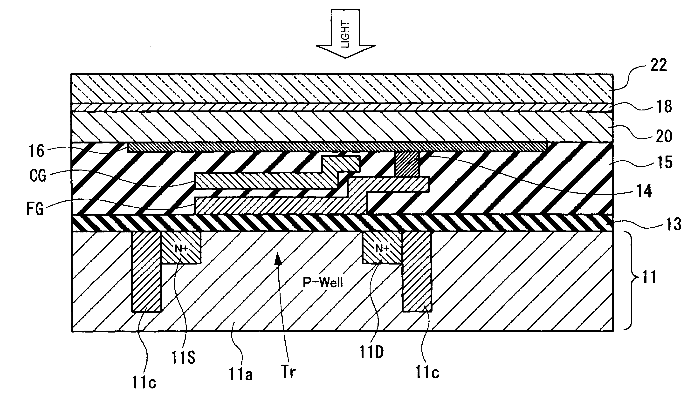
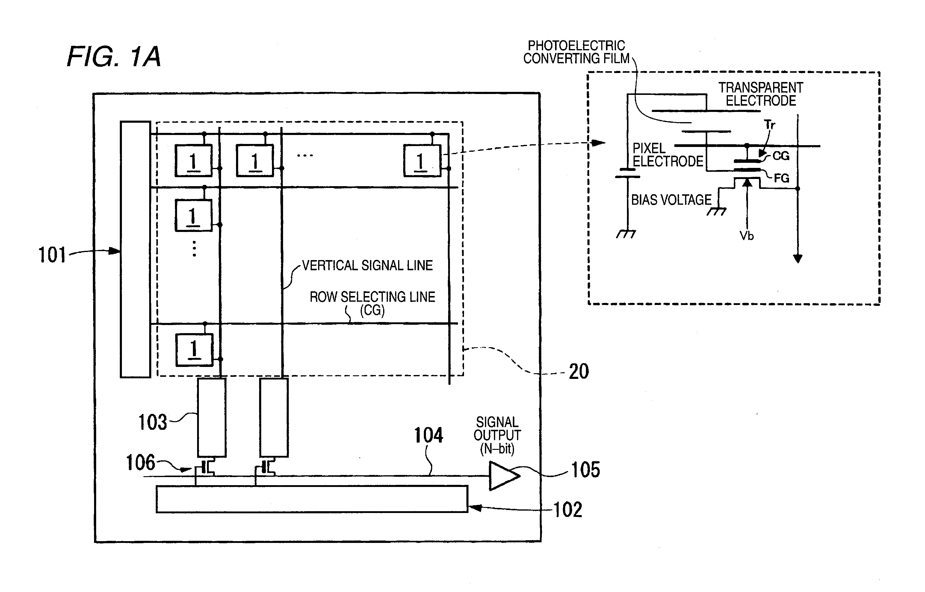
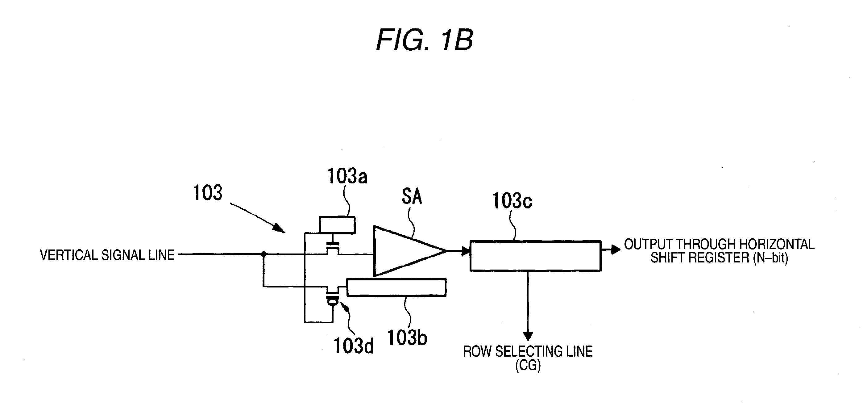
[0031]An embodiment according to the invention will be described below in detail with reference to the drawings. FIG. 1A is a typical diagram showing a structure of an embodiment of an imaging device. FIG. 1B is a circuit diagram showing a reading circuit. The imaging device has a large number of pixel portions 1 disposed in a matrix on a surface of a semiconductor substrate. At a light incident side of the large number of pixel portions 1, a photoelectric converting film 20 is provided to cover all of the pixel portions 1.

[0032]FIG. 1A shows an equivalent circuit for one of the pixel portions. Each of the pixel portions includes a transistor Tr having a single MOS type structure. A floating gate (hereinafter referred to as an FG) connected electrically to the photoelectric converting film 20 and a control gate (hereinafter referred to as a CG) functioning as a gate of the transistor Tr are formed in each of the pixel portions 1. A source of the transistor Tr is grounded. The transi...


PUM


Abstract

An imaging device includes: a semiconductor substrate; a photoelectric converting film that is forms on the semiconductor substrate and that generates charges corresponding to an incident light; a plurality of pixel portions that receive the charges from the photoelectric converting film, a floating gate that is electrically connected to the photoelectric converting film; and a transistor that fluctuates a threshold voltage so as to start to increase a drain current when an electric potential of the floating gate changes.

Description

CROSS-REFERENCE TO RELATED APPLICATIONS[0001]The present application claims priority from Japanese Patent Application No. 2008-222742 filed on Aug. 29, 2008 and Japanese Patent Application No. 2009-197753 filed on Aug. 28, 2009; the entire content of which is incorporated herein by reference.BACKGROUND OF INVENTION[0002]1. Field of the Invention[0003]The present invention relates to an imaging device including a photoelectric converting film, a method of driving the imaging device, and an imaging apparatus.[0004]2. Description of the Related Art[0005]Examples of an imaging device include a CMOS type image sensor and an interline CCD type image sensor. The imaging device has a plurality of photodiodes arranged on a semiconductor substrate, and each of the photodiodes constitutes each pixel portion. An opening formed on a metal shielding film is provided on the photodiode of the pixel portion, and a microlens for collecting an incident light onto the photodiode is provided on a light ...

Claims


Application Information

Patent Timeline
Patent Type & Authority Applications(United States)
IPC IPC(8): H04N5/335H01L27/14H01L27/146H04N5/361H04N5/369H04N5/3745
CPCH01L27/14609H01L27/14621H04N2209/047H04N5/3745H04N9/045H04N5/361H04N25/63H04N25/77H04N25/134
Inventor SIZUKUISI, MAKOTO
Owner FUJIFILM CORP
Why Eureka
Try Eureka