Thin film field-effect transistor and display using the same

a field-effect transistor and thin film technology, applied in the direction of semiconductor devices, electrical devices, semiconductor/solid-state device details, etc., can solve the problems of difficult high-refined patterning, difficult direct formation of thin films on resin substrates that are low in heat resistance, and complicated processes, so as to achieve strong bonding force

Active Publication Date: 2010-03-11
SAMSUNG DISPLAY CO LTD
View PDF0 Cites 96 Cited by
  • Summary
  • Abstract
  • Description
  • Claims
  • Application Information

AI Technical Summary

Problems solved by technology

However, manufacture of the above transistors using silicon thin films requires a thermal process of relatively high temperature, and it is generally difficult to directly form a thin film on a resin substrate that is low in heat resistance.
However, an amorphous oxide semiconductor layer is liable to cause oxygen defects, and has problems such that the layer fluctuates according to the atmosphere at the time of film forming, semiconductor characteristics are variable due to plasma irradiation and the like at the time of film forming, or performances fluctuate during storage after manufacture.
Further, there is a problem such that an amorphous oxide semiconductor layer is liable to be corroded by an acidic etchant for patterning, and a patterning process by photolithography cannot be used, so that highly refined patterning is difficult.
However, since both methods require exact control of process conditions in the control of oxygen defects, the processes are complicated, the apparatus are large-sized, and strong heat treatment cannot be applied to a TFT using a film (flexible) substrate.
Further, the problems of etchant-resistance in a patterning process and storage stability of a semiconductor film after manufacture remain unresolved.

Method used


Image

  • Thin film field-effect transistor and display using the same
  • Thin film field-effect transistor and display using the same
  • Thin film field-effect transistor and display using the same

Examples


example 1

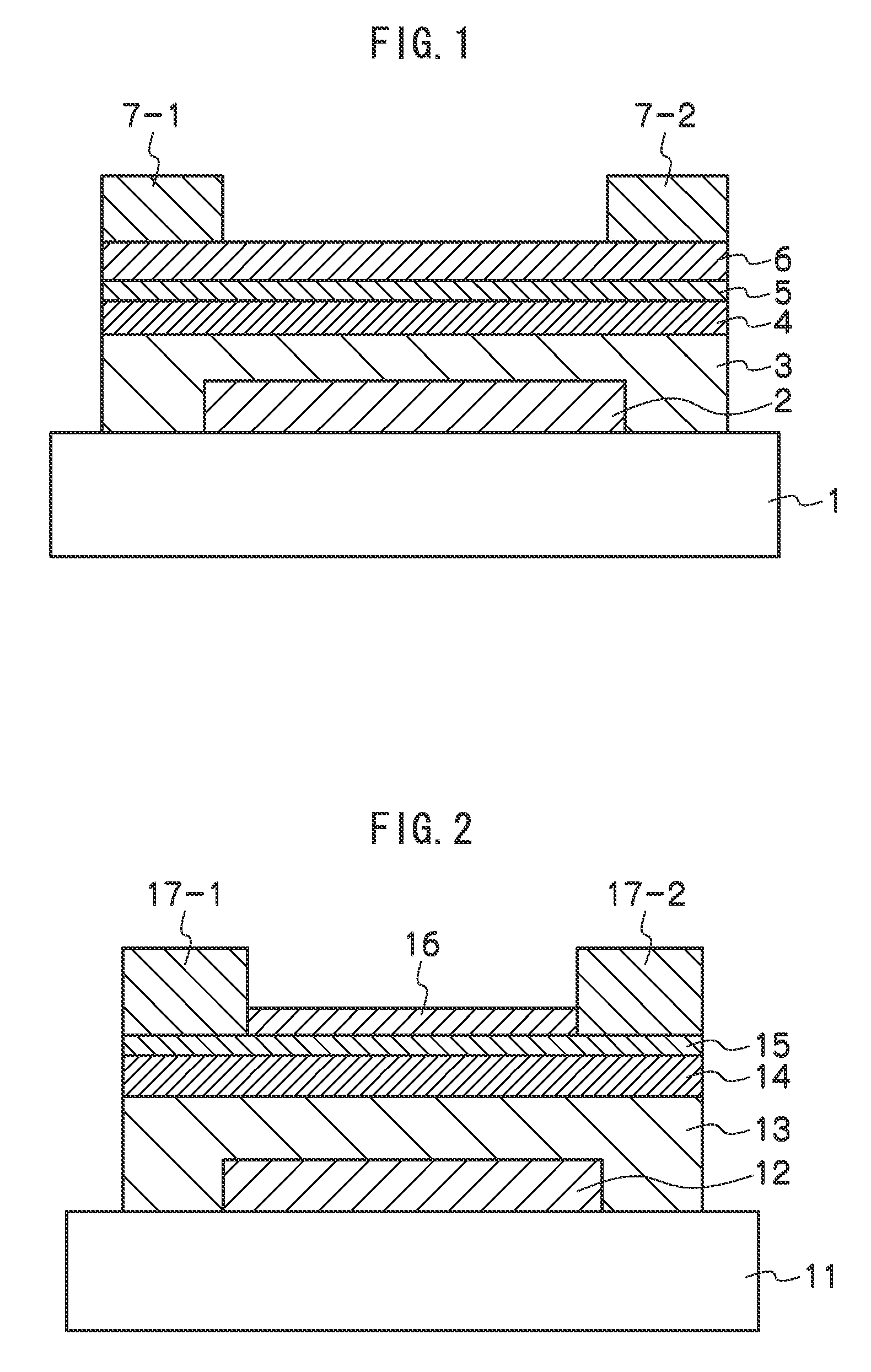
[0277]1. Manufacture of TFT Device

[0278]1) Manufacture of TFT Device 1 of the Invention

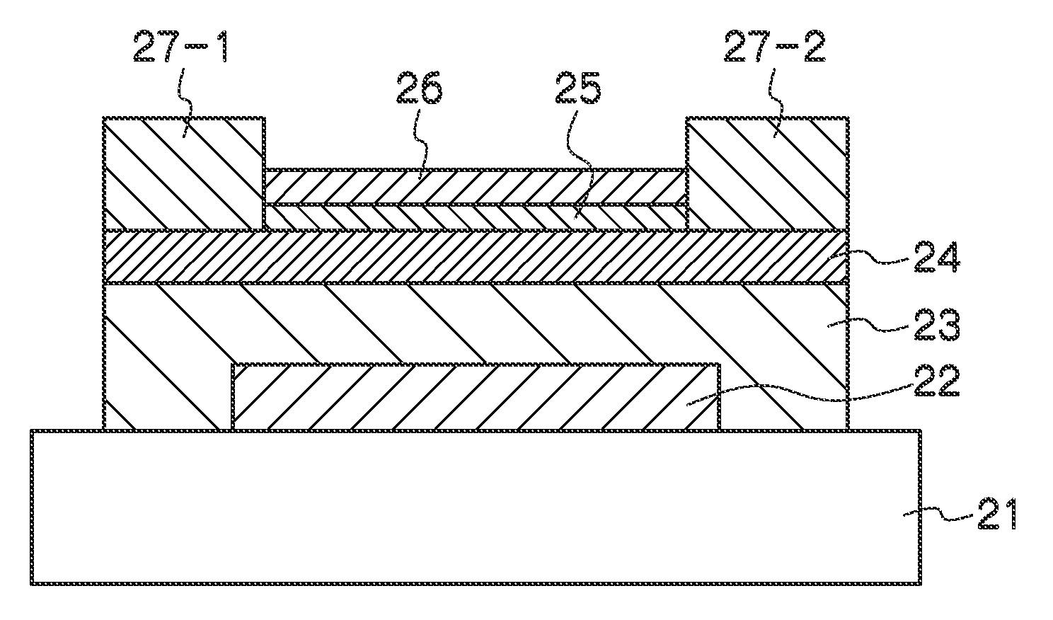
[0279]TFT device having the cross sectional structure shown in FIG. 2 was manufactured.

[0280]As a substrate, non-alkali glass plate (product No. 1737, manufactured by Corning Inc.) was used. The substrate was subjected to ultrasonic wave washing with pure water for 15 minutes, with acetone for 15 minutes, and with pure water for 15 minutes in order. An ITO thin film (thickness: 30 nm) as a gate electrode was formed on the substrate by using indium tin oxide (ITO) target containing 10 mass % of SnO2 (indium / tin=95 / 5 in a molar ratio) according to RF magnetron sputtering (conditions of a film-forming temperature: 43° C., sputtering gas Ar: 12 sc cm, RF power: 40 W, film-forming pressure: 0.4 Pa). In patterning of the gate electrode ITO, a shadow mask was used at the time of sputtering.

[0281]In the next place, the following gate insulating film was formed on the gate electrode.

[0282]A gate insulating...

example 2

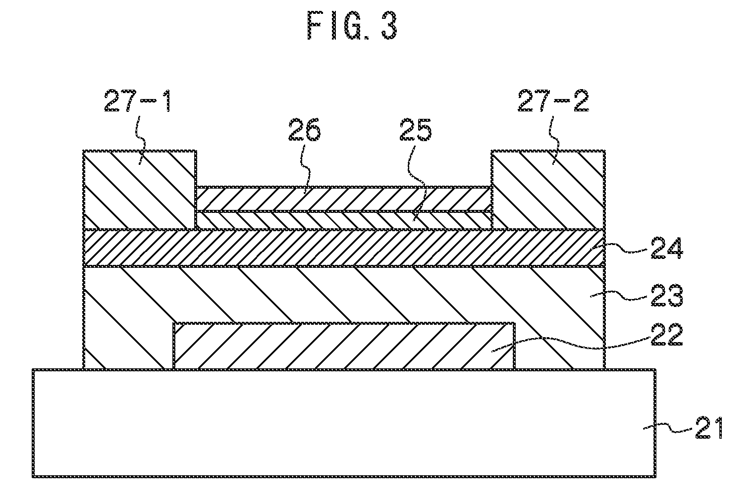
[0332]1. Manufacture of TFT Device 6 of the Invention

[0333]TFT device 6 of the invention was manufactured in the same manner as in the manufacture of TFT device 1 of the invention except for using, as the substrate, a film with a barrier having an insulating layer having the following barrier function on both surfaces of a polyethylene naphthalate film, and changing the gate electrode formed on the barrier film from 30 nm of ITO to 40 nm of Mo. Film-forming conditions of Mo were the same as in Example 1.

[0334]SiON was used as the insulating layer having a barrier function. The film-forming conditions of the insulating layer SiON are as follows. Insulating layer: SiON is deposited in a thickness of 500 nm. An RF magnetron sputtering deposition method is used in deposition of SiON (conditions of sputtering: target, Si3N4, RF power: 400 W, flow rate of Ar / O2=12 / 3 sc cm, film-forming pressure: 0.45 Pa).

[0335]2. Evaluation of Performances

[0336]As a result of evaluation of the performance...


PUM


Abstract

The present invention provides a thin film field-effect transistor comprising a substrate having thereon at least a gate electrode, a gate insulating film, an active layer, a source electrode, and a drain electrode, wherein the active layer is an oxide semiconductor layer, a resistance layer having an electric conductivity that is lower than an electric conductivity of the active layer is provided between the active layer and at least one of the source electrode or the drain electrode, and an intermediate layer comprising an oxide comprising an element having a stronger bonding force with respect to oxygen than that of the oxide semiconductor in the active layer is provided between the active layer and the resistance layer.

Description

CROSS-REFERENCE TO RELATED APPLICATION[0001]This application claims priority under 35 USC 119 from Japanese Patent Application No. 2008-231101 filed on Sep. 9, 2008, the disclosure of which is incorporated by reference herein.BACKGROUND[0002]1. Field of the Invention[0003]The present invention relates to a thin film field-effect transistor and a display using the same. Specifically, the invention relates to a thin film field-effect transistor using an amorphous oxide semiconductor in an active layer and a display using the same.[0004]2. Related Art[0005]In recent years, due to progress in liquid crystal and electroluminescence (EL) technologies and the like, flat panel displays (FPD) have been put to practical use. In particular, since high intensity light emission can be obtained by low voltage with an organic electroluminescent device (hereinafter sometimes also referred to as “an organic EL device”) using a thin film material that is excited and emits light by applying an electri...

Claims


Application Information

Patent Timeline
Patent Type & Authority Applications(United States)
IPC IPC(8): H01L29/786
CPCH01L29/78609H01L29/78696H01L29/7869H01L29/78621
Inventor ITAI, YUICHIRO
Owner SAMSUNG DISPLAY CO LTD
Why Eureka
Try Eureka