High-color-temperature tandem white OLED

Active Publication Date: 2010-03-18
GLOBAL OLED TECH
View PDF18 Cites 34 Cited by
  • Summary
  • Abstract
  • Description
  • Claims
  • Application Information

AI Technical Summary

Benefits of technology

[0014]It is an advantage of this invention that it provides an OLED display with an im

Problems solved by technology

This produces manufacturing difficulties.
However, it is difficult to achieve light emission with strong intensity in the red, green, and blue portion

Method used


Image

  • High-color-temperature tandem white OLED
  • High-color-temperature tandem white OLED
  • High-color-temperature tandem white OLED

Examples


example 1

Comparative

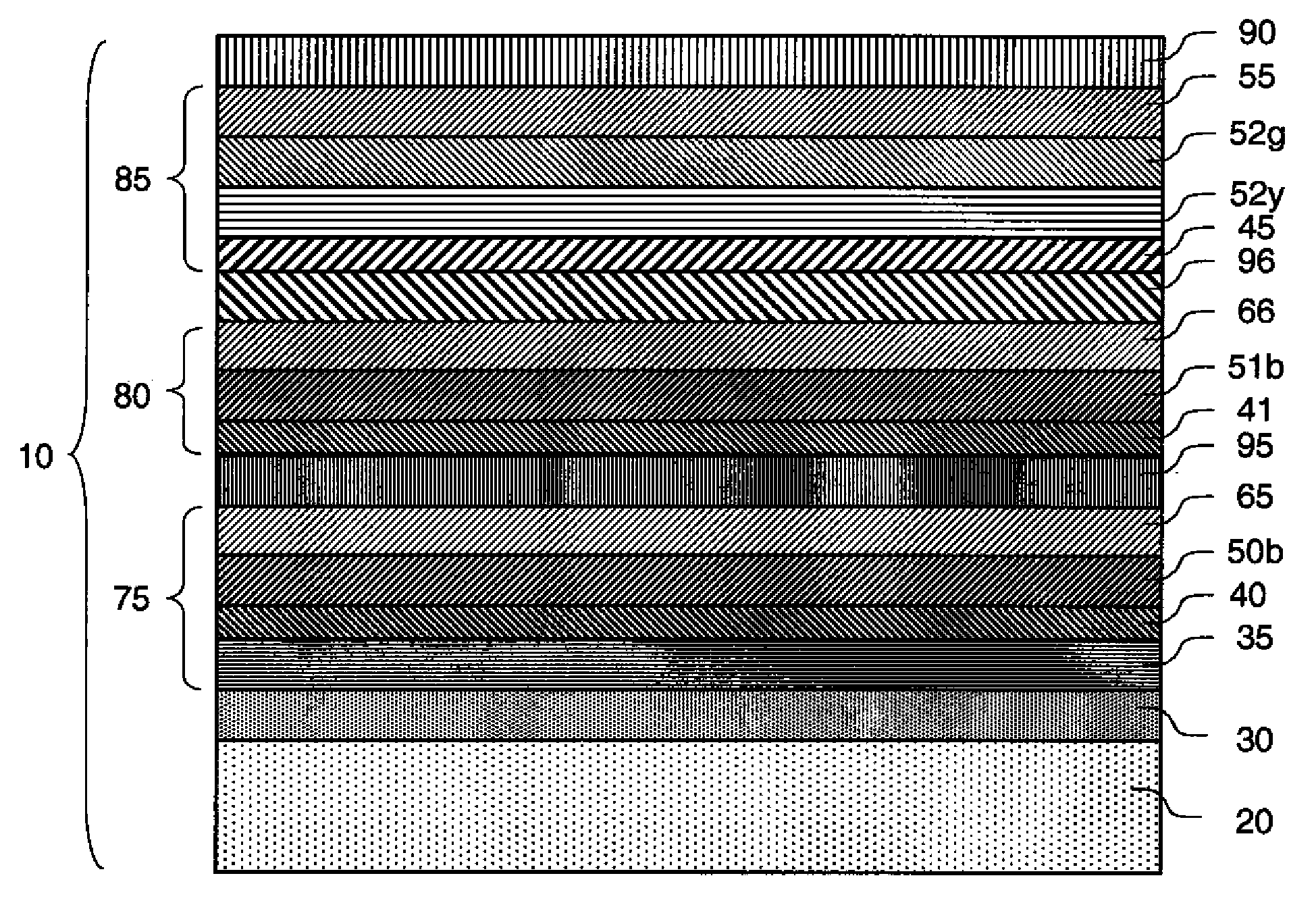
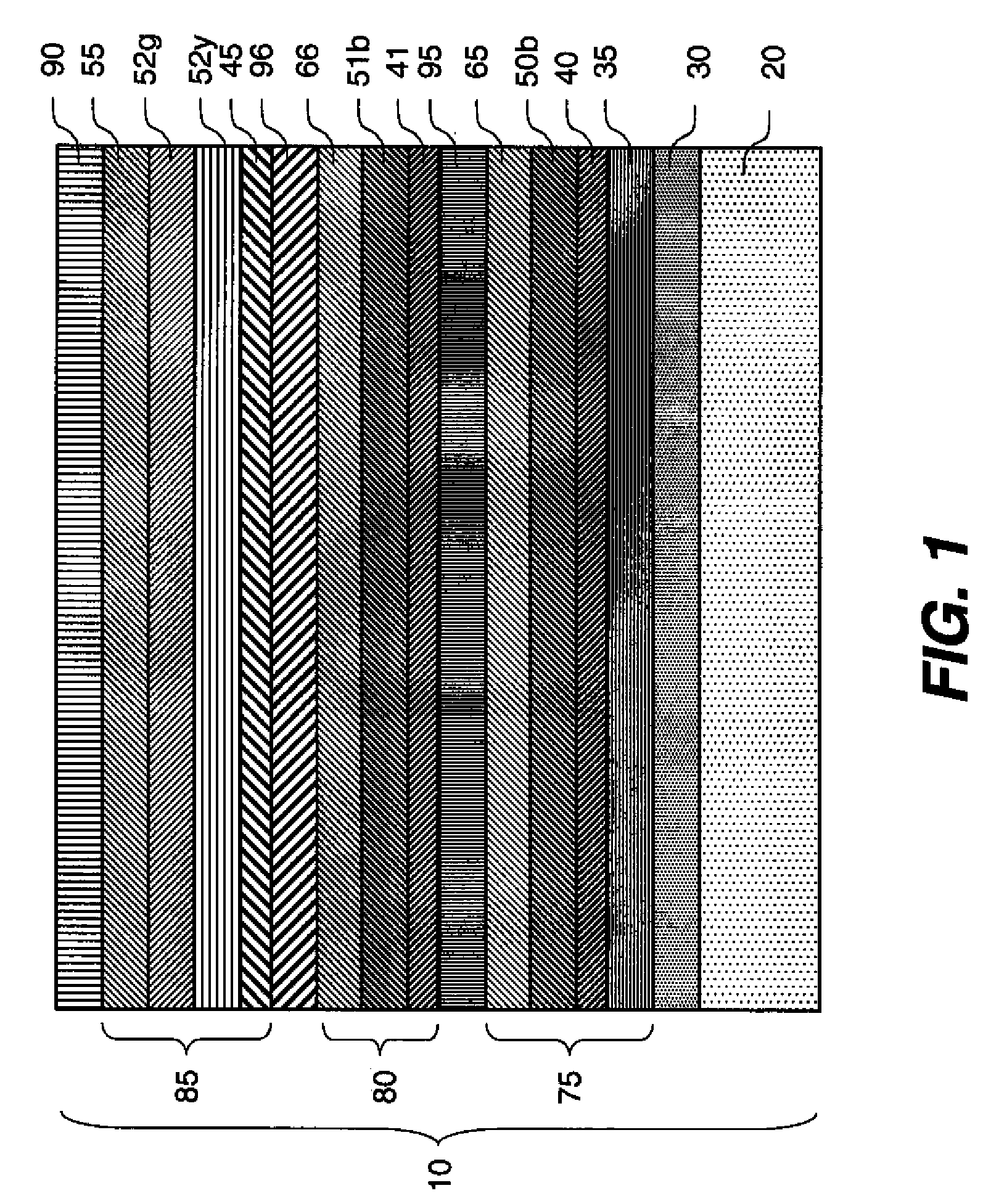
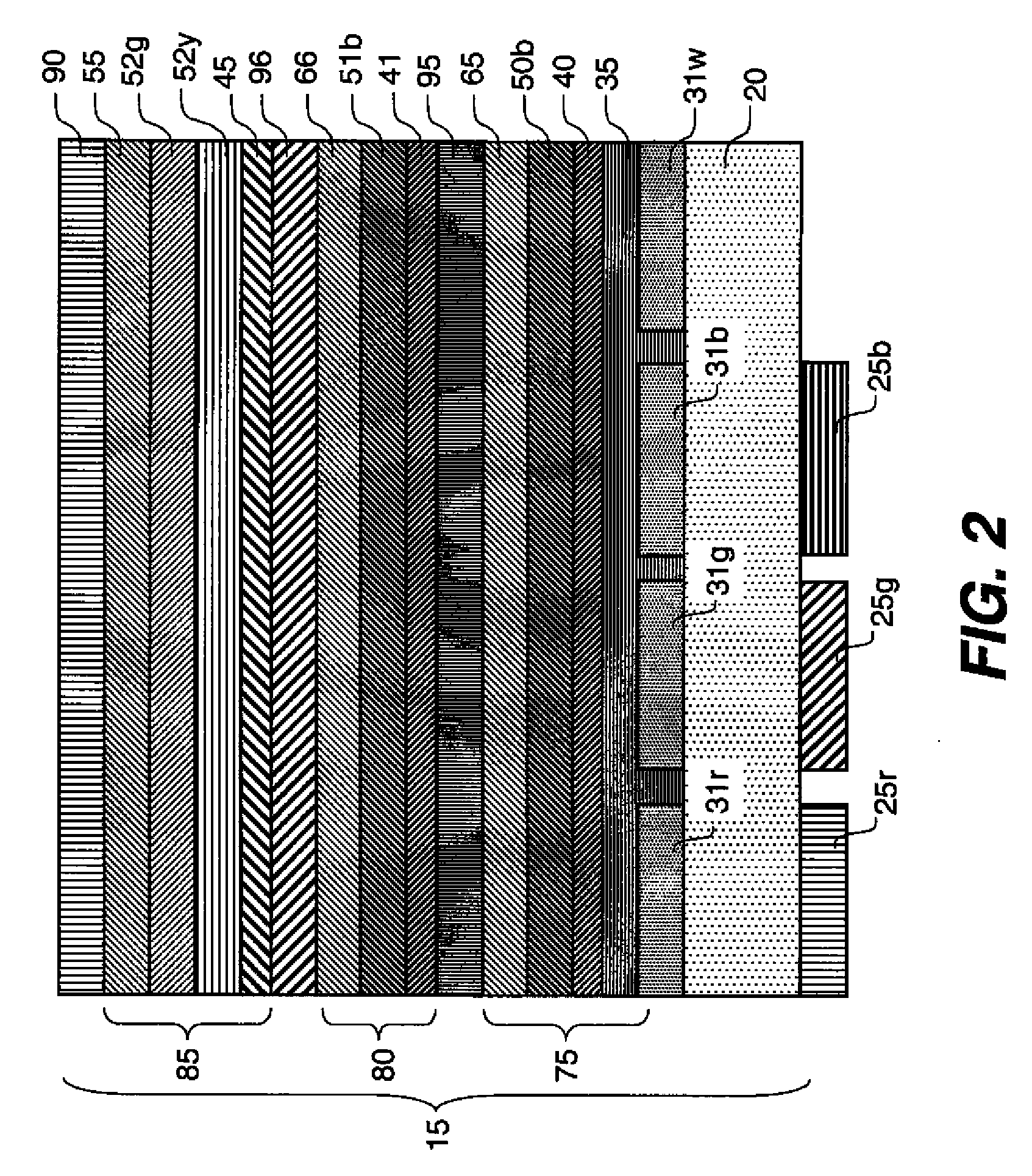
[0098]1. A clean glass substrate was deposited by sputtering with indium tin oxide (ITO) to form a transparent electrode of 60 nm thickness.[0099]2. The above-prepared ITO surface was treated with a plasma oxygen etch.[0100]3. The above-prepared substrate was further treated by vacuum-depositing a 1 nm layer of hexacyanohexaazatriphenylene (CHATP) as a hole-injecting layer (HIL).

[0101]4. The above-prepared substrate was further treated by vacuum-depositing a 130 nm layer of 4,4′-bis[N-(1-naphthyl)-N-phenylamino]biphenyl (NPB) as a hole-transporting layer (HTL).[0102]5. The above-prepared substrate was further treated by vacuum-depositing a 20 nm yellow light-emitting layer including 48% NPB (as host) and 50% 9-(1-naphthyl)-10-(2-naphthyl)anthracene (NNA) as a co-host with 2% yellow-orange emitting dopant diphenyltetra-t-butylrubrene (PTBR).

[0103]6. The above-prepared substrate was further treated by vacuum-depositing a 20 nm blue light-emitting layer including 85% NNA hos...

example 2

Inventive

[0113]1. A clean glass substrate was deposited by sputtering with indium tin oxide (ITO) to form a transparent electrode of 60 nm thickness.[0114]2. The above-prepared ITO surface was treated with a plasma oxygen etch.[0115]3. The above-prepared substrate was further treated by vacuum-depositing a 10 nm layer of CHATP as a hole-injecting layer (HIL).[0116]4. The above-prepared substrate was further treated by vacuum-depositing a 163 nm layer of NPB as an HTL.[0117]5. The above-prepared substrate was further treated by vacuum-depositing a 30 nm blue light-emitting layer including 95% NNA host with 5% BED-1 as blue-emitting dopant.[0118]6. A 40 nm mixed electron-transporting layer was vacuum-deposited, including 49% Bphen and 49% (8-quinolinolato)lithium (LiQ) as co-hosts, with 2% Li metal.[0119]7. The above-prepared substrate was further treated by vacuum-depositing a 10 nm layer of CHATP as a p-type doped organic layer (HIL).[0120]8. The above-prepared substrate was further...

example 3

Inventive

[0129]An OLED device was constructed as described above for Example 2 except that the hole-transporting layer thicknesses were varied as follows:[0130]4. The above-prepared substrate was further treated by vacuum-depositing a 200 nm layer of NPB as an HTL.[0131]8: The above-prepared substrate was further treated by vacuum-depositing a 10 nm layer of NPB as an HTL.[0132]12. The above-prepared substrate was further treated by vacuum-depositing a 20 nm layer of NPB as an HTL.


PUM


Abstract

An OLED device having two spaced electrodes including: first, second, and third light-emitting units disposed between the electrodes, the first light-emitting unit produces light that has multiple peaks at wavelengths longer than 500 nm and substantially no emission at wavelengths shorter than 480 nm, and the second and third light-emitting units produce light that has substantial emission at wavelengths shorter than 500 nm; intermediate connectors respectively disposed between the first and second light-emitting units, and between the second and third light-emitting units; and wherein the OLED device emits light with a color temperature greater than 7,000K.

Description

CROSS REFERENCE TO RELATED APPLICATIONS[0001]Reference is made to commonly assigned U.S. Pat. No. 7,332,860, entitled EFFICIENT WHITE-LIGHT OLED DISPLAY WITH FILTERS by Hatwar et al.; U.S. patent application Ser. No. 11 / 749,883, entitled HYBRID OLED WITH FLUORESCENT AND PHOSPHORESCENT LAYERS by Deaton et al.; and U.S. patent application Ser. No. 11 / 749,899, entitled HYBRID FLUORESCENT / PHOSPHORESCENT OLEDS by Deaton et al.; the disclosures of which are incorporated herein by reference.FIELD OF THE INVENTION[0002]The present invention relates to broadband light-producing OLED displays suitable for large displays.BACKGROUND OF THE INVENTION[0003]An organic light-emitting diode device, also called an OLED, commonly includes an anode, a cathode, and an organic electroluminescent (EL) unit sandwiched between the anode and the cathode. The organic EL unit includes at least a hole-transporting layer (HTL), a light-emitting layer (LEL), and an electron-transporting layer (ETL). OLEDs are att...

Claims


Application Information

Patent Timeline
IPC IPC(8): H01J1/63
CPCH01L51/5036H01L51/5278H01L51/0085H01L51/0054H01L51/0072H01L51/0059H10K85/622H10K85/631H10K85/6572H10K85/342H10K50/125H10K50/19H10K50/12H10K50/11
Inventor SPINDLER, JEFFREY P.HATWAR, TUKARAM K.
Owner GLOBAL OLED TECH
Why Eureka
Try Eureka