Photoelectric conversion device and manufacturing method thereof

a technology of conversion device and photoelectric technology, which is applied in the manufacture of final products, basic electric elements, climate sustainability, etc., can solve the problems of double steps and inability to obtain conversion efficiency equivalent to that of single crystal silicon in which a small number of defects exist, and achieve the effect of improving conversion efficiency and improving light collection efficiency

Inactive Publication Date: 2010-03-25
SEMICON ENERGY LAB CO LTD
View PDF32 Cites 6 Cited by
  • Summary
  • Abstract
  • Description
  • Claims
  • Application Information

AI Technical Summary

Benefits of technology

[0021]The second semiconductor layer including the single crystal region and the amorphous region is provided between the first semiconductor layer having one conductivity type and the third semiconductor layer having a conductivity type opposite to the one conductivity type, whereby light collection efficiency is improved and conversion efficiency can be increased.
[0022]The semiconductor layer including the single crystal region and the amorphous region is formed over the buffer layer including the single crystal region and the amorphous region, so that the photoelectric conversion device which allows the best use of a synergistic effect of a single crystal semiconductor and an amorphous semiconductor can be manufactured without increase of the manufacturing steps.

Problems solved by technology

However, in the conventional tandem photoelectric conversion device in which a single crystal semiconductor and an amorphous semiconductor are combined, there is a problem in that a top photoelectric conversion cell and a bottom photoelectric conversion cell need to be manufactured independently and therefore, steps are doubled.
On the other hand, in the i-type layer in which a microcrystalline silicon layer and an amorphous silicon layer are stacked, a large number of defects exist in the microcrystalline silicon layer; therefore, conversion efficiency equivalent to that of single crystal silicon in which a small number of defects exist cannot be obtained.

Method used


Image

  • Photoelectric conversion device and manufacturing method thereof
  • Photoelectric conversion device and manufacturing method thereof
  • Photoelectric conversion device and manufacturing method thereof

Examples


example 2

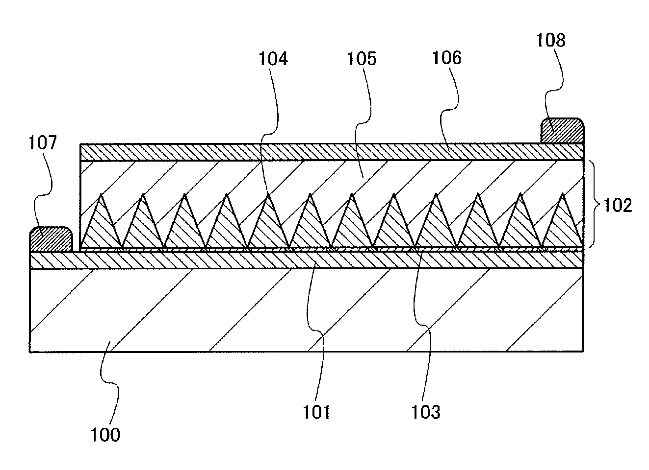
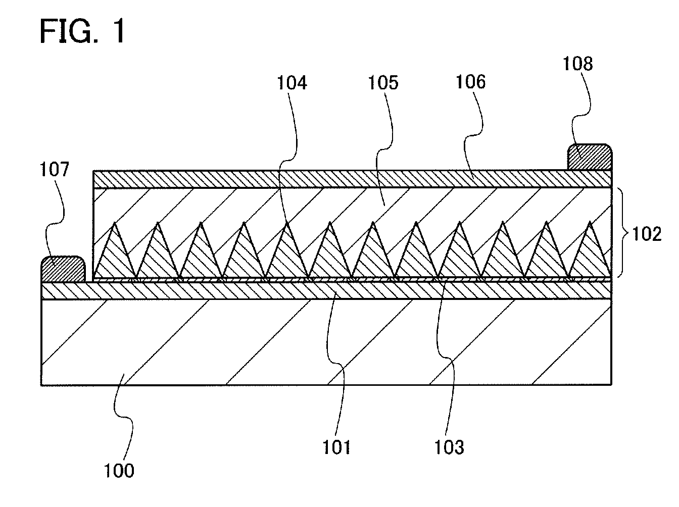
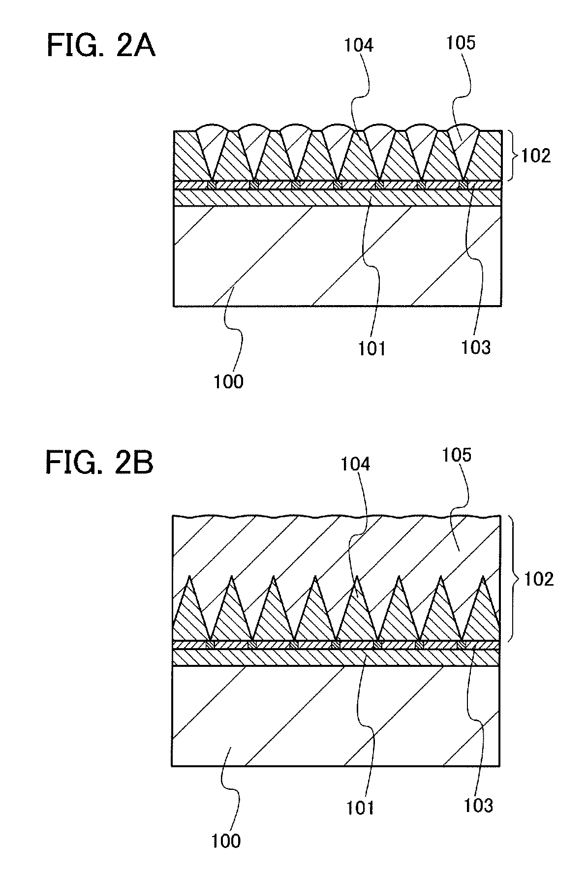
[0114]In this example, an example is described, in which a single crystal silicon layer is formed over a glass substrate and a semiconductor layer including a single crystal region and an amorphous region is formed thereover.

[0115]An n-type single crystal silicon wafer which had a (100) plane and resistivity of 3 Ωcm to 7 Ωcm and which had been subjected to mirror polishing was used. The single crystal silicon wafer was thermally oxidized by heating at 950° C. in an oxygen atmosphere including HCl at 3% and an oxide film with a thickness of 500 nm was formed thereover.

[0116]The single crystal silicon wafer over which the oxide film was formed was irradiated with hydrogen ions, so that a damaged layer was formed in the single crystal silicon wafer. The irradiation with hydrogen ions was performed at an accelerating voltage of 25 kV and dosage of 1.8×10¹⁶ ions / cm2.

[0117]After that, a silicon nitride oxide film was formed by a plasma CVD method so as to have a thickness of 50 nm over t...


PUM


Abstract

An object is to increase conversion efficiency of a photoelectric conversion device without increase in the manufacturing steps. The photoelectric conversion device includes a first semiconductor layer formed using a single crystal semiconductor having one conductivity type which is formed over a supporting substrate, a buffer layer including a single crystal region and an amorphous region, a second semiconductor layer which includes a single crystal region and an amorphous region and is provided over the buffer layer, and a third semiconductor layer having a conductivity type opposite to the one conductivity type, which is provided over the second semiconductor layer. A proportion of the single crystal region is higher than that of the amorphous region on the first semiconductor layer side in the second semiconductor layer, and the proportion of the amorphous region is higher than that of the single crystal region on the third semiconductor layer side.

Description

BACKGROUND OF THE INVENTION[0001]1. Field of the Invention[0002]An embodiment of the present invention relates to a structure of a photoelectric conversion device utilizing photoelectric effect of a semiconductor and a manufacturing method thereof.[0003]2. Description of the Related Art[0004]A photoelectric conversion device in which a photoelectric conversion cell formed using a single crystal semiconductor and a photoelectric conversion cell formed using an amorphous semiconductor are combined is known. For example, a tandem photoelectric conversion device is disclosed, which is formed as follow: a p-type single crystal silicon layer separated from a p-type single crystal silicon substrate is bonded to a substrate; and an n-type single crystal silicon layer, a p-type amorphous silicon layer, and an n-type amorphous silicon layer are formed in this manner over the p-type single crystal silicon layer (see Patent Document 1).[0005]On the other hand, a single-type photoelectric conver...

Claims


Application Information

Patent Timeline
Patent Type & Authority Applications(United States)
IPC IPC(8): H01L31/0248H01L31/18
CPCH01L21/0237H01L21/02532H01L21/0262H01L21/02636H01L31/036H01L31/077H01L31/1804Y02E10/548Y02E10/547H01L31/20H01L31/0376H01L31/075Y02P70/50
Inventor KATO, SHOHIURA, YOSHIKAZUSHIMOMURA, AKIHISAOHTSUKI, TAKASHITORIUMI, SATOSHIARAI, YASUYUKI
Owner SEMICON ENERGY LAB CO LTD
Why Eureka
Try Eureka