Substrate structure with die embedded inside and dual build-up layers over both side surfaces and method of the same

a technology of substrate structure and die, which is applied in the direction of semiconductor devices, semiconductor/solid-state device details, electrical devices, etc., can solve the problems of time-consuming manufacturing process, inability to meet the demand of producing smaller chips with high-density elements on the chip, and complicated semiconductor devices

Active Publication Date: 2010-03-25
YANG CHING LUNG
View PDF3 Cites 178 Cited by
  • Summary
  • Abstract
  • Description
  • Claims
  • Application Information

AI Technical Summary

Benefits of technology

[0007]For the aforementioned, the present invention provides a substrate structure which has embedded dice inside with stress buffer properties a

Problems solved by technology

As a semiconductor become more complicated, the traditional package technique, for example lead frame package, flex package, rigid package technique, can't meet the demand of producing smaller chip with high density elements on the chip.
Therefore, these techniques are time consuming for manufacturing process.
Since the chip package technique is highly influenced by the development of integrated circuits, therefore, as the size of electronics has become demanding, so does the package technique.
Though the advantages of WLP technique mentioned above, some issues still exist influencing the acceptance of WLP technique.
For instance, the CTE difference (mismatching) between the materials of a structure of WLP and the mother board (PCB) becomes another critical factor t

Method used


Image

  • Substrate structure with die embedded inside and dual build-up layers over both side surfaces and method of the same
  • Substrate structure with die embedded inside and dual build-up layers over both side surfaces and method of the same
  • Substrate structure with die embedded inside and dual build-up layers over both side surfaces and method of the same

Examples


Embodiment Construction

[0036]The invention will now be described in greater detail with preferred embodiments of the invention and illustrations attached. Nevertheless, it should be recognized that the preferred embodiments of the invention is only for illustrating. Besides the preferred embodiment mentioned here, present invention can be practiced in a wide range of other embodiments besides those explicitly described, and the scope of the present invention is expressly not limited expect as specified in the accompanying Claims.

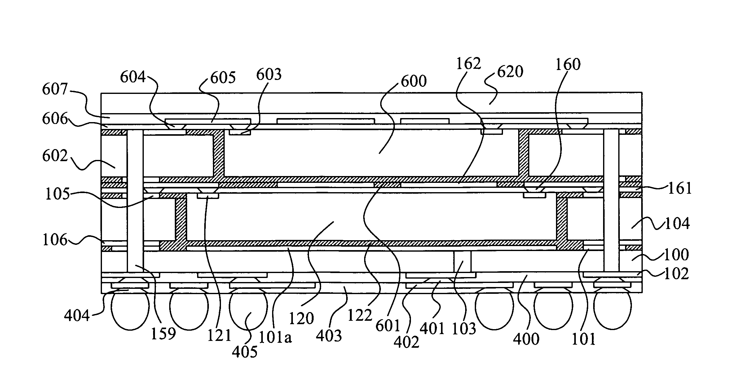
[0037]The present invention discloses a substrate structure with die (or multi-chips) embedded and dual build-up layers formed over the both side-surfaces, shown in FIG. 12, and it illustrates a cross sectional view of system in package (SIP) structure which includes a substrate having die embedded inside with double side build up layers and passive components, WL-CSP, CSP, BGA, Flip Chip etc. surface mounting on top build up layers and terminal pins on opposite side according to ...


PUM


Abstract

The present invention discloses a structure of device package comprising a first substrate with a die metal pad, a first wiring circuit on top surface of said first substrate and a second wiring circuit on bottom surface of said first substrate. A die is disposed on the die metal pad. A second substrate has a die opening window for receiving the die, a third wiring circuit on top surface of the second substrate and a fourth wiring circuit on bottom surface of the second substrate. An adhesive material is filled into the gap between back side of the die and top surface of the first substrate and between the side wall of the die and the side wall of the die receiving through hole and the bottom side of the second substrate.

Description

FIELD OF THE INVENTION [0001]This invention relates to a substrate structure with embedded dice inside to form panel level packaging, and more particularly to a fan-out panel level package with dual build up layers formed over the both side-surfaces to improve the reliability and to reduce the device size, especially in thickness.DESCRIPTION OF THE PRIOR ART [0002]In the field of semiconductor devices, the device density is increased and the device dimension is reduced, continuously. The demand for the packaging or interconnecting techniques in such high density devices is also increased to fit the situation mentioned above. Conventionally, in the flip-chip attachment method, an array of solder bumps is formed on the surface of the die. The formation of the solder bumps may be carried out by using a solder composite material through a solder mask for producing a desired pattern of solder bumps. The function of chip package includes power distribution, signal distribution, heat dissi...

Claims


Application Information

Patent Timeline
IPC IPC(8): H01L23/52H01L21/00
CPCH01L23/49816H01L23/5384H01L2924/10253H01L23/5389H01L24/18H01L24/82H01L2224/18H01L2224/82039H01L2924/01013H01L2924/01029H01L2924/01075H01L2924/01078H01L2924/01079H01L2924/01082H01L2924/09701H01L2924/14H01L2924/15311H01L2924/19041H01L2924/19043H01L2924/01006H01L2924/01033H01L2924/01047H01L2924/014H01L2224/16225H01L2924/00H01L21/568H01L24/19H01L2224/04105H01L2224/05001H01L2224/05008H01L2224/05009H01L2224/05024H01L2224/05026H01L2224/05124H01L2224/05144H01L2224/05147H01L2224/05155H01L2224/05166H01L2224/05569H01L2224/12105H01L2224/13025H01L2224/16227H01L2224/16235H01L2224/32225H01L2224/32245H01L2224/73267H01L2224/92244H01L2924/19105H01L2924/351H01L2924/3511H01L2924/3512H01L2924/00014
Inventor YANG, WEN-KUN
Owner YANG CHING LUNG
Why Eureka
Try Eureka