Semiconductor device

a technology of semiconductor devices and semiconductors, applied in semiconductor devices, semiconductor/solid-state device details, instruments, etc., can solve the problems of increasing communication distance, reducing the power consumption and and the inability to find the means to solve these problems, so as to improve the speed performance of the entire system and reduce power consumption

Inactive Publication Date: 2010-04-01
HITACHI LTD
View PDF17 Cites 52 Cited by
  • Summary
  • Abstract
  • Description
  • Claims
  • Application Information

AI Technical Summary

Benefits of technology

[0007]Under the background art described above, the present inventors contemplate that in order to achieve further improvement of performance, reduction of power consumption, and increase in space efficiency, it is effective to stack a plurality of processor LSIs in conjunction with and in addition to a plurality of memory LSIs.
[0008]However, the present inventors have found a problem that increasing the number of stacked layers will result in an increase in communication distance even when the communication is in the stacking direction, and performing frequent data transmission between stacked LSIs over multiple layers will degrade the power consumption and speed performance of the entire system.
[0012]According to the present invention, it becomes possible to reduce the power consumption and to improve the speed performance of the entire system in the stack of LSIs.

Problems solved by technology

However, the present inventors have found a problem that increasing the number of stacked layers will result in an increase in communication distance even when the communication is in the stacking direction, and performing frequent data transmission between stacked LSIs over multiple layers will degrade the power consumption and speed performance of the entire system.
However, means for solving these problems cannot be found in JP Patent Publication (Kokai) No. 2002-231880 described above.

Method used


Image

  • Semiconductor device
  • Semiconductor device
  • Semiconductor device

Examples


example 1

(Configuration)

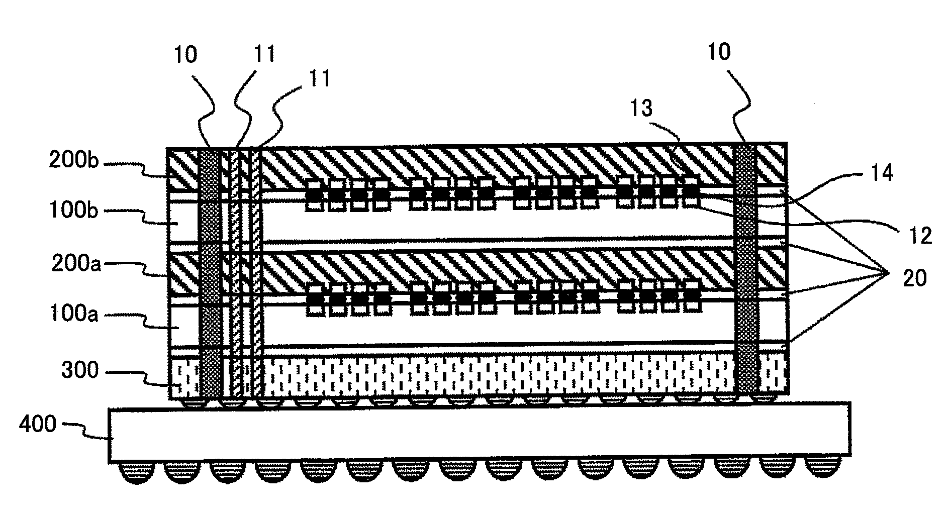
[0068]FIG. 1 is a stack sectional view to show the semiconductor device relating to a first embodiment according to the present invention. In the present embodiment, a memory LSI 200 mounted with a memory for storing data and a processor LSI 100 mounted with an arithmetic unit are stacked in such a way that respective surfaces on which circuitry is disposed face each other. A pad 12 on the processor LSI 100 and a pad 13 on the memory LSI 200 are electrically connected with a solder bump 14. Two sets of combinations of such processor LSI 100 and memory LSI 200, that is, a combination of a processor LSI 100a and a memory LSI 200a and a combination of a processor LSI 100b and a memory LSI 200b are stacked. An interface LSI 300 is stacked in the underlying layer, and the entire structure is stacked on a package board 400. Further, the present embodiment includes a through silicon via for power supply 10 for providing power supply to each LSI and a through silicon via for ...

example 2

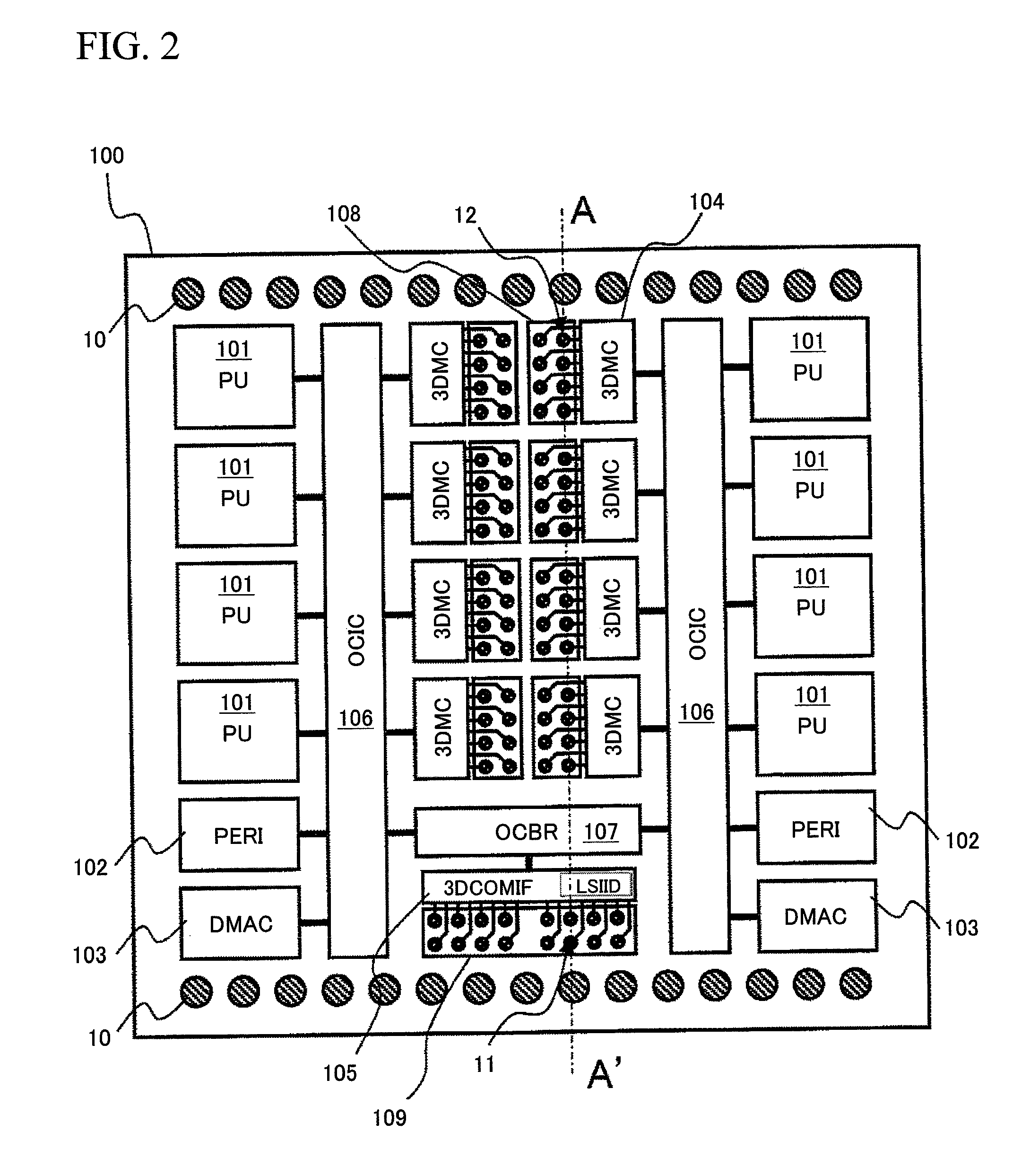
[0133]FIG. 10 is a stack sectional view of the semiconductor device relating a second embodiment of the present invention, in contrast with FIG. 1. In FIG. 10, like parts corresponding to those of FIG. 1 are given like reference characters and detailed description thereof will not be repeated. In FIG. 10, a stacked LSI system is configured such that a processor LSI 100a, a processor LSI 100b, and a processor LSI 100c are stacked respectively interposing a memory LSI 200a and a memory LSI 200b therebetween, and an interface LSI 300 and a package board 400 are stacked in the underlying layer of those stacked five LSIs. Moreover, in FIG. 10, the processor LSIs 100a, 100b and 100c are electrically connected with the memory LSIs 200a and 200b through a TSV block for memory access 18.

[0134]FIG. 11 shows the connection configuration between the processor LSIs 100a, 100b and 100c and the memory LSIs 200a and 200b in more detail. Through silicon vias 181a to 181c, 182a to 182c, 183a to 183c,...


PUM


Abstract

In a semiconductor device in which a plurality of memory LSIs and a plurality of processor LSIs are stacked, as the number of stacked layers increase, the communication distance of data between a memory LSI and a processor LSI will increase. Therefore, the parasitic capacitance and parasitic resistance of the wiring used for the communication increase and, as a result of which, the power and speed performance of the entire system will be degraded. At least two or more of the combinations of a processor LSI 100 and a memory LSI 200 are stacked and the processor LSI 100 and the memory LSI 200 in the same combination are stacked adjacent to each other in the vertical direction. Communication between the processor LSI 100 and the memory LSI 200 in the same combination is performed by a dedicated electrode provided therebetween, and communication between processor LSIs 100 and communication from the processor LSI 100 to the outside are performed by a through silicon via for signal 11 which passes through all the LSIs.

Description

CLAIM OF PRIORITY[0001]The present application claims priority from Japanese patent application JP 2008-249496 filed on Sep. 29, 2008, the content of which is hereby incorporated by reference into this application.BACKGROUND OF THE INVENTION[0002]1. Field of the Invention[0003]The present invention relates to a semiconductor device in which a plurality of LSIs are stacked.[0004]2. Background Art[0005]So far, with the advancement of microfabrication technology, the performance improvement and functional upgrade of LSIs have been achieved by integrating more transistors in a single chip. However, due to the effects of the limits of miniaturization and the increases in the cost of utilizing state-of-the-art processes, performance improvement by means of integration into a single chip as practiced so far may not be a best solution in the future. Accordingly, three-dimensional integration by stacking a plurality of LSIs will be a promising technology. With this being the case, communicat...

Claims


Application Information

Patent Timeline
Patent Type & Authority Applications(United States)
IPC IPC(8): H01L25/16H01L23/538
CPCG11C5/02H01L2225/06558G11C5/063H01L23/544H01L23/552H01L25/0657H01L25/18H01L2223/54433H01L2223/5444H01L2223/54473H01L2224/16145H01L2224/73207H01L2224/73253H01L2224/73265H01L2225/0651H01L2225/06513H01L2225/06527H01L2225/06541H01L2924/01057H01L2224/48227H01L2924/15311G11C5/04H01L2224/05571H01L2924/00014H01L2224/0554H01L2224/05599H01L2224/05099H01L2224/0555H01L2224/0556
Inventor ITO, KIYOTOSAEN, MAKOTOKURODA, YUKI
Owner HITACHI LTD
Why Eureka
Try Eureka