Nano-crystal diamond film, manufacturing method thereof, and device using nano-crystal diamond film

a nano-crystal diamond and nano-crystal technology, applied in the direction of thermoelectric device junction materials, chemically reactive gases, chemical vapor deposition coatings, etc., can solve the problems of high rough surface of diamond film, inability to employ a substrate which is suited for forming diamond films of large area at low cost, and all conventional diamond films are not suited for practical us

Inactive Publication Date: 2010-04-08
TOPPAN PRINTING CO LTD +1
View PDF4 Cites 48 Cited by
  • Summary
  • Abstract
  • Description
  • Claims
  • Application Information

AI Technical Summary

Benefits of technology

[0016]According to a second aspect of the present invention, there is proposed an electrochemical device comprising one or more pairs of electrodes to detect the kind of test substance to be measured by taking advantage of a redox reaction of a surface of electrodes and to measure the concentration of the test substance, wherein at least one of the electrodes comprises a substrate, and the aforementioned nano-crystal diamond film formed on a surface of the substrate.
[0017]According to a third aspect of the present invention, there is proposed an electrochemical electrode to be employed as an anode and / or a cathode for electrolyzing liquid or gas by taking advantage of an electrochemical reaction, wherein the anode and / or the cathode comprises a substrate, and the aforementioned nano-crystal diamond film is formed on a surface of the substrate.

Problems solved by technology

However, since the diamond film to be obtained is a polycrystal, the surface of diamond film is highly rough.
Therefore, it is impossible to employ a substrate which is suited for forming a diamond film of large area at low cost such as a glass substrate or a polymer substrate to be used for a display for example.
As described above, all of the conventional diamond films are not suited for practical use because of the cost of the substrate material and of the difficulties to increase the size thereof.
However, no one has succeeded, as yet, in discovering such a film and a method of forming such a film.

Method used


Image

  • Nano-crystal diamond film, manufacturing method thereof, and device using nano-crystal diamond film
  • Nano-crystal diamond film, manufacturing method thereof, and device using nano-crystal diamond film
  • Nano-crystal diamond film, manufacturing method thereof, and device using nano-crystal diamond film

Examples


example 1

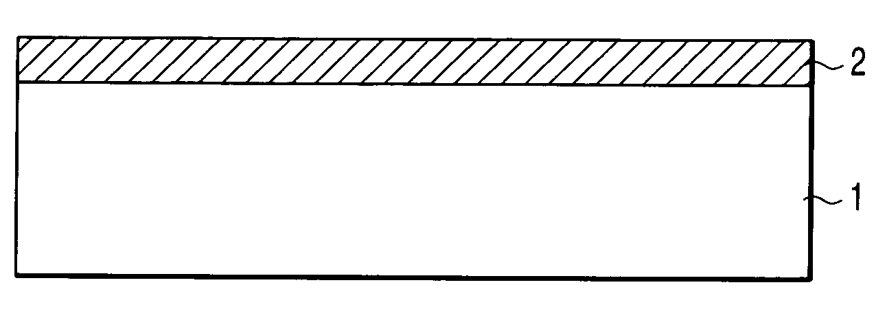
[0180]As shown in FIG. 11A, by making use of a microwave plasma CVD apparatus, a nano-crystal diamond film 122 was formed on a monocrystalline silicon substrate 121 having a thickness of 525 μm.

[0181]The conditions for the microwave plasma CVD were as follows.

[0182]Raw gas: methane (flow rate: 2 sccm) and hydrogen (flow rate: 18 sccm)

[0183]Doping gas: hydrogen sulfide (0.01 to 5 vol % based on the raw gas)

[0184]Temperature of substrate: 500° C.

[0185]Reaction pressure: 5 Torr

[0186]MW power: 500 W

[0187]By means of the microwave plasma CVD and under the aforementioned conditions, a nano-crystal diamond film 122 having a thickness of 500 nm was formed. Upon finishing the formation of the film, the surface of the nano-crystal diamond film 122 was subjected to a hydrogen plasma treatment for 5 minutes.

[0188]When the nano-crystal diamond film 122 thus manufactured was observed by means of a transmission electron microscope (TEM), it was possible to confirm a crystal grain diameter of the o...

example 2

[0190]As shown in FIG. 11B, by making use of a microwave plasma CVD apparatus, a nano-crystal diamond film 132 was formed on a glass substrate 131 having a thickness of 1.1 mm.

[0191]The conditions for the microwave plasma CVD were as follows.

[0192]Raw gas: methane (flow rate: 2 sccm) and hydrogen (flow rate: 18 sccm)

[0193]Doping gas: hydrogen sulfide (0.01 to 5 vol % based on the raw gas)

[0194]Temperature of substrate: 300° C.

[0195]Reaction pressure: 5 Torr

[0196]MW power: 500 W

[0197]By means of the microwave plasma CVD and under the aforementioned conditions, a nano-crystal diamond film 132 having a thickness of 500 nm was formed. Upon finishing the formation of the film, the surface of the nano-crystal diamond film 132 was subjected to a hydrogen plasma treatment for 5 minutes.

[0198]As a result, it was possible to obtain a nano-crystal diamond film 132 having almost the same features as those obtained in Example 1 even in this example.

example 3

[0199]As shown in FIG. 11C, by making use of a microwave plasma CVD apparatus, a nano-crystal diamond film 142 was formed on a polymer substrate 141 having a thickness of 1 mm.

[0200]The conditions for the microwave plasma CVD were as follows.

[0201]Raw gas: methane (flow rate: 2 sccm) and hydrogen (flow rate: 18 sccm)

[0202]Doping gas: hydrogen sulfide (0.01 to 5 vol % based on the raw gas)

[0203]Temperature of substrate: 100° C.

[0204]Reaction pressure: 5 Torr

[0205]MW power: 200 W

[0206]By means of the microwave plasma CVD and under the aforementioned conditions, a nano-crystal diamond film 142 having a thickness of 300 nm was formed. Upon finishing the formation of the film, the surface of the nano-crystal diamond film 142 was subjected to a hydrogen plasma treatment for 5 minutes.

[0207]As a result, it was possible to obtain a nano-crystal diamond film 142 having almost the same features as those obtained in Example 1 even in this example.

[0208]Next, examples related to various applica...


PUM

PropertyMeasurementUnit
grain diameteraaaaaaaaaa
surface flatnessaaaaaaaaaa

Abstract

A nano-crystal diamond film synthesized on a substrate and containing, as a major component, nano-crystal diamond having a grain diameter from 1 nm to less than 1000 nm. This nano-crystal diamond film can be formed on a substrate by means of a plasma CVD method using a raw material gas containing a hydrocarbon and hydrogen, allowing the formation of the nano-crystal diamond film to take place outside the plasma region. This nano-crystal diamond film is applicable to the manufacture of an electrochemical device, an electrochemical electrode, a DNA chip, an organic electroluminescent device, an organic photoelectric receiving device, an organic thin film transistor, a cold electron-emission device, a fuel cell and a catalyst.

Description

CROSS REFERENCE TO RELATED APPLICATIONS[0001]This is a Continuation Application of PCT Application No. PCT / JP2004 / 007642, filed May 27, 2004, which was published under PCT Article 21(2) in Japanese.[0002]This application is based upon and claims the benefit of priority from prior Japanese Patent Application No. 2002-344066, filed Nov. 27, 2002, the entire contents of which are incorporated herein by reference.BACKGROUND OF THE INVENTION[0003]1. Field of the Invention[0004]This invention relates to a nano-crystal diamond film formed of fine diamond crystal of the order of nanometers. This invention also relates to a method of manufacturing such a nano-crystal diamond film and to various kinds of devices using such a nano-crystal diamond film.[0005]2. Description of the Related Art[0006]A type of diamond in which carbon atoms are bonded to each other through covalent bond by way of sp3 hybrid orbital is widely known to have, due to its high bonding energy, specific physical properties...

Claims


Application Information

Patent Timeline
Patent Type & Authority Applications(United States)
IPC IPC(8): H01L51/10H01M4/86C23C16/44B32B5/16G01N27/26G01N33/48H01L31/00B01J21/18G03F7/00B32B37/00H01L51/52C23C16/27C30B25/02C30B25/10C30B29/04C30B29/60
CPCC23C16/27C23C16/278C30B25/105C30B29/04C30B29/605H01L21/0237Y10T156/10H01L21/02573H01L21/02595H01L21/0262H01L29/1602Y10T428/25H01L21/02527C30B25/165H01L33/02
Inventor GAMO, HIDENORIANDO, TOSHIHIRO
Owner TOPPAN PRINTING CO LTD
Why Eureka
Try Eureka