Esd-protection device, a semiconductor device and integrated system in a package comprising such a device

a protection device and semiconductor technology, applied in the direction of semiconductor devices, diodes, electrical apparatus, etc., can solve the problem of still relatively high clamping voltage, and achieve the effect of optimizing performan

Active Publication Date: 2010-04-08
NEXPERIA BV
View PDF5 Cites 11 Cited by
  • Summary
  • Abstract
  • Description
  • Claims
  • Application Information

AI Technical Summary

Benefits of technology

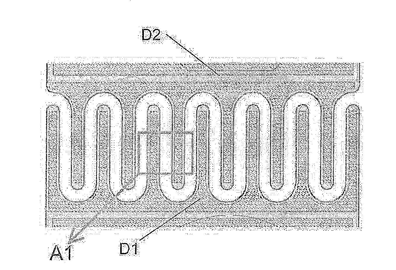
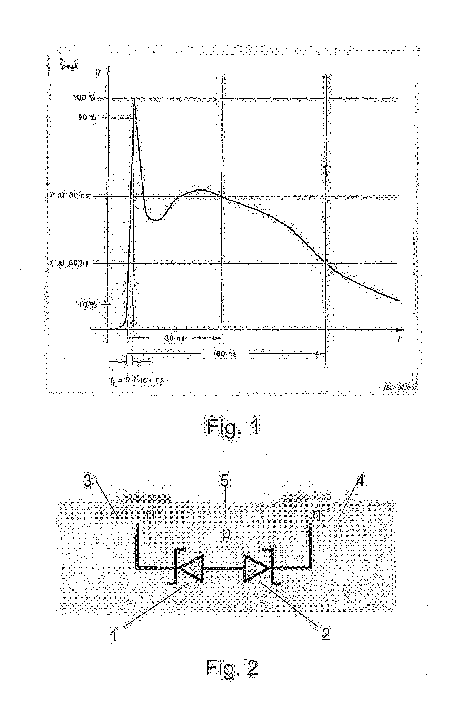
[0033]In a suitable embodiment, the trench diodes comprise a first region of a first conductivity type at a sidewall of the trench and a second region of a second opposite conductivity type adjacent to the first region away from the trench. This embodiment allows that the second regions of the first and second arrays of trench diodes are formed by one a single region. In this embodiment, the size of this second region may be tuned so as to create a bipolar transistor, as described above. While the provision of such bipolar transistor in addition to the anti-series arrangement of the trench diodes is considered to give optimal performance, this bipolar transistor is not strictly necessary for all applications. Particularly, the ESD protection will already benefit from the structure with the said first and second array of trench diodes, for instance to create a back-to-back diode with an gigantic junction area within a small substrate area of the substrate.
[0034]As explained above, one advantage of this embodiment is the provision of trench capacitors in series with the trench diodes. The trench capacitors are then defined between the contact and the first region of the diodes. Such trench capacitors may be applied for filtering purposes, without hampering the ESD-performance of the trench diodes. Effectively, therefore, the capacitors can be defined as well, when no filter performance is desired.
[0035]A further advantage of such embodiment is that trench capacitors may further be defined in an area of the substrate remote from the present arrays of trench diodes. Such trench capacitors can be made within the same process flow, without the need of temporarily covering the trenches. These capacitors will be functionally independent, and may be used, for example, as decoupling capacitors for RF applications, or as part of DC-DC converters.

Problems solved by technology

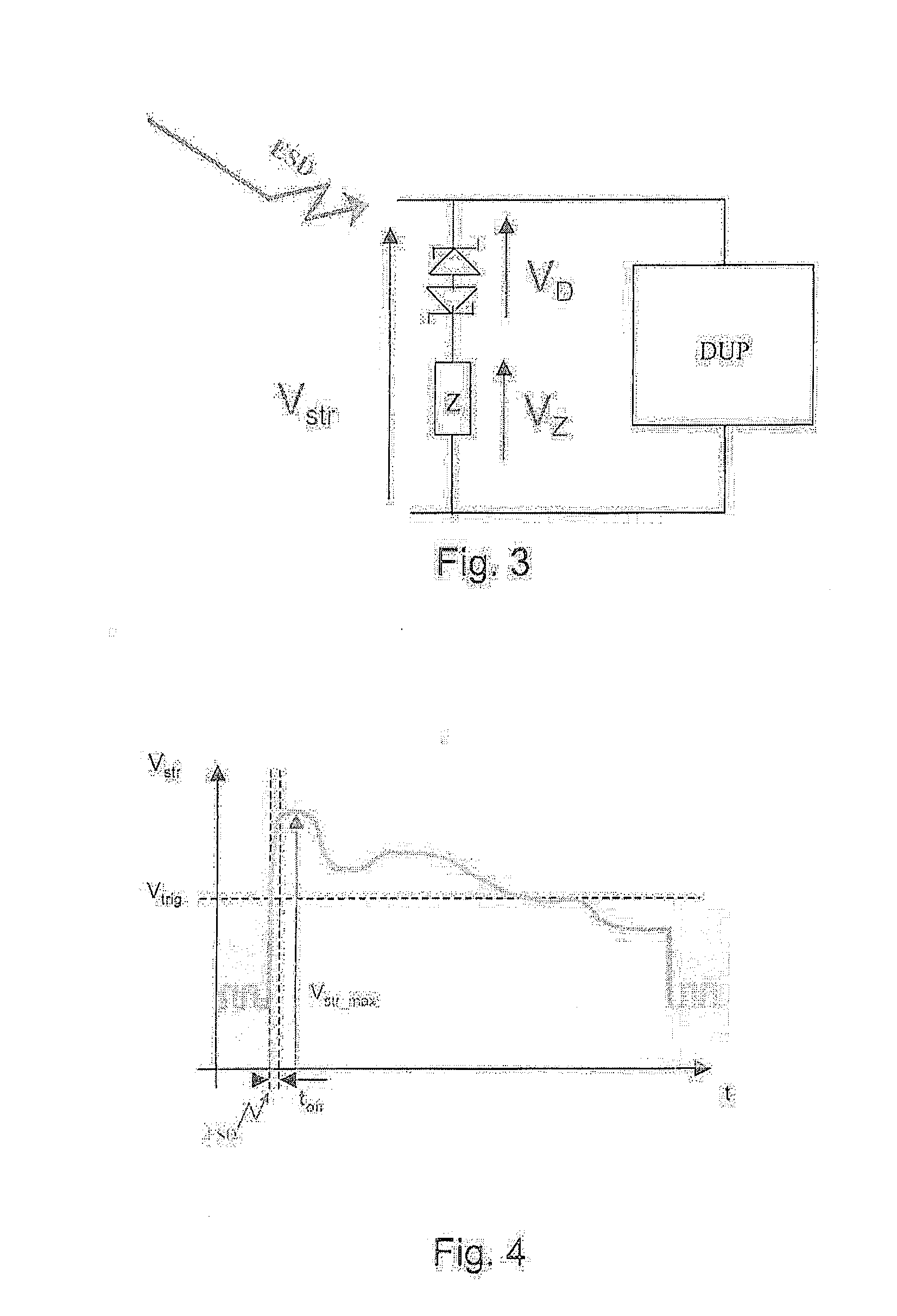
A disadvantage of the known ESD protection devices is that the clamping voltage is still relatively high.

Method used


Image

  • Esd-protection device, a semiconductor device and integrated system in a package comprising such a device
  • Esd-protection device, a semiconductor device and integrated system in a package comprising such a device
  • Esd-protection device, a semiconductor device and integrated system in a package comprising such a device

Examples


Embodiment Construction

[0056]It should be noted that the above-mentioned embodiments illustrate rather than limit the invention, and that those skilled in the art will be able to design many alternative embodiments without departing from the scope of the appended claims. In the claims, any reference signs placed between parentheses shall not be construed as limiting the claim. Use of the verb “comprise” and its conjugations does not exclude the presence of elements or steps other than those stated in a claim. The article “a” or “an” preceding an element does not exclude the presence of a plurality of such elements. The invention may be implemented by means of hardware comprising several distinct elements, and by means of a suitably programmed computer. In the device claim enumerating several means, several of these means may be embodied by one and the same item of hardware. The mere fact that certain measures are recited in mutually different dependent claims does not indicate that a combination of these ...


PUM


Abstract

The invention relates to an ESD protection device comprising: a first contact (10) and a second contact (20), and an electrical node (12); a bipolar transistor (6) having a base, an emitter, and a collector, the base and emitter forming a base-emitter junction, the base and collector forming a base-collector junction, the emitter being connected to the first contact (10), the collector being connected to the second contact (20), the base being connect to the electrical node (12); a first diode (1) connected between the electrical node (12) and the first contact (10), the first diode (1) comprising a first junction arranged in the same direction as the base-emitter junction, and—a second diode (2) connected between the electrical node (12) and the second contact (20), in anti-series with the first diode (1) on a path from the first contact (10) to the second contact (20), the second diode (2) comprising a second junction arranged in the same direction as the base-collector junction, wherein the bipolar transistor (6) is dimensioned to have such a current gain (β) that the voltage-current characteristic of the ESD protection device, measured between the first (10) and second contact (20), exhibits a voltage snap-back effect (SNP) at its trigger voltage (Vtrig). The voltage snap-back effect (SNP) results in a lower clamping voltage of the ESD protection device. The invention further relates a semiconductor device and an integrated system in a package comprising said ESD protection device.

Description

FIELD OF THE INVENTION[0001]The invention relates to an ESD protection device, a semiconductor device and an integrated system in a package comprising such a device.BACKGROUND OF THE INVENTION[0002]ESD protection devices of the kind mentioned in the opening paragraph are known, for example from a Philips product data sheet of the PESDxL2BT series (Rev. 01—1 Nov. 2005), “Low capacitance double bidirectional ESD protection diodes in SOT23”. This datasheet discloses a low capacitance double bidirectional Electrostatic Discharge (ESD) protection diodes in a SOT23 small Surface Mounted Device (SMD) plastic package designed to protect two signal lines from the damage caused by ESD and other transients. The package comprises three pins (“cathode 1”, “cathode 2”, “double cathode 3”). Between pins “cathode 1” and “double cathode 3” there is a first anti-series connection of two Zener-diodes, and between pins “cathode 2” and “double cathode 3” there is a second anti-series connection of two Z...

Claims


Application Information

Patent Timeline
Patent Type & Authority Applications(United States)
IPC IPC(8): H02H9/00
CPCH01L29/861H01L27/0255
Inventor SAVIN, EMMANUELBOUVIER, STEPHANE
Owner NEXPERIA BV
Why Eureka
Try Eureka