

Method of manufacturing nitride semiconductor light emitting element and nitride semiconductor light emitting element
- Summary
- Abstract
- Description
- Claims
- Application Information
AI Technical Summary
Benefits of technology
Problems solved by technology
Method used
Image

Examples
embodiment 1
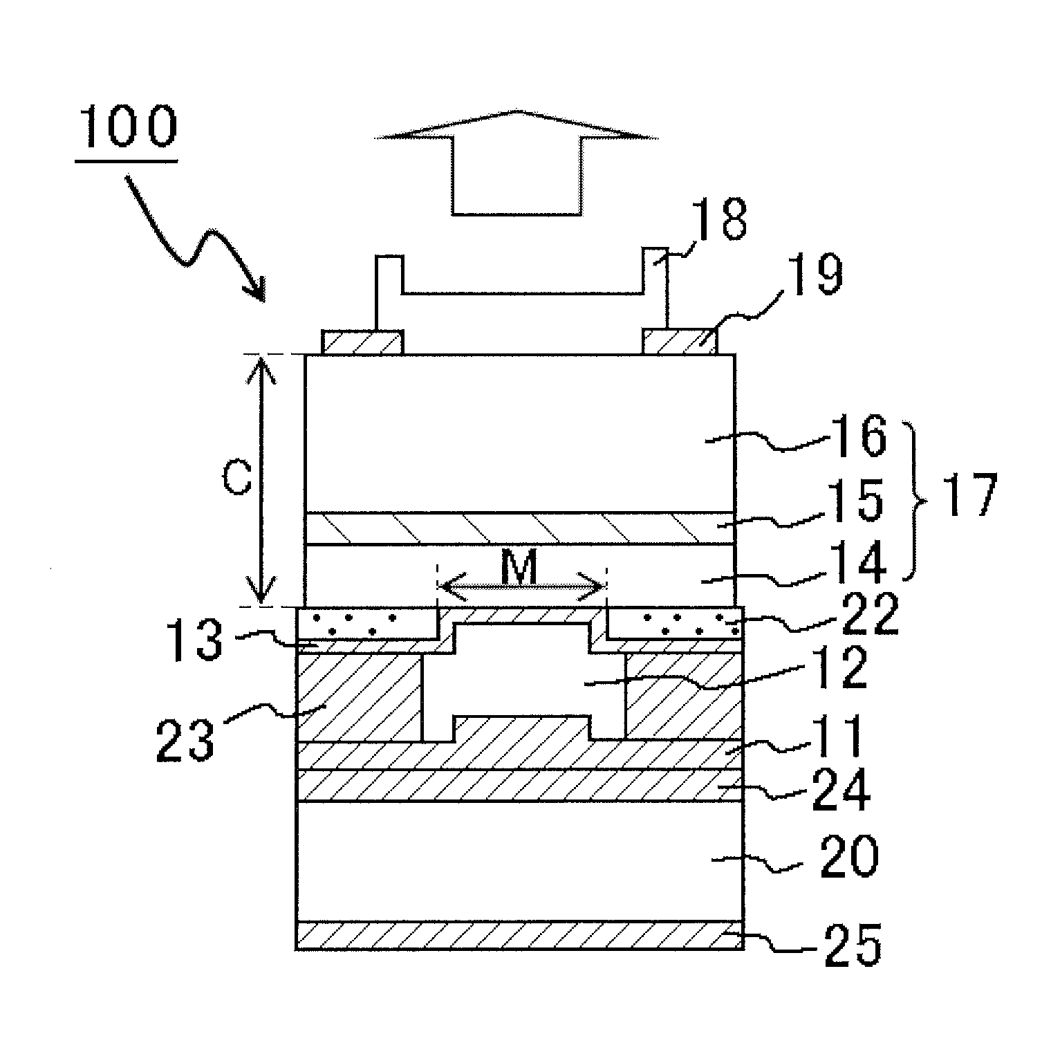
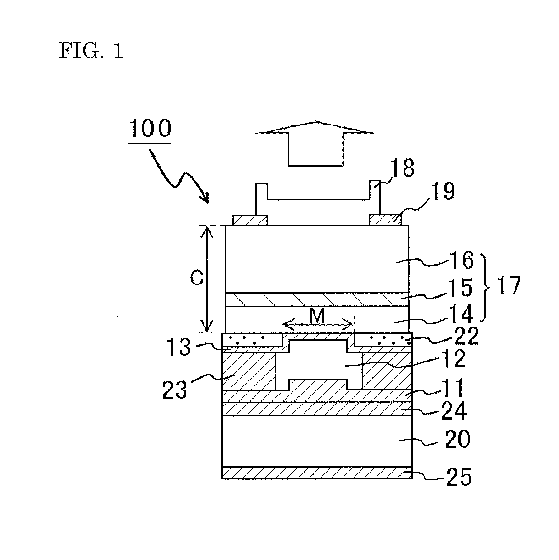
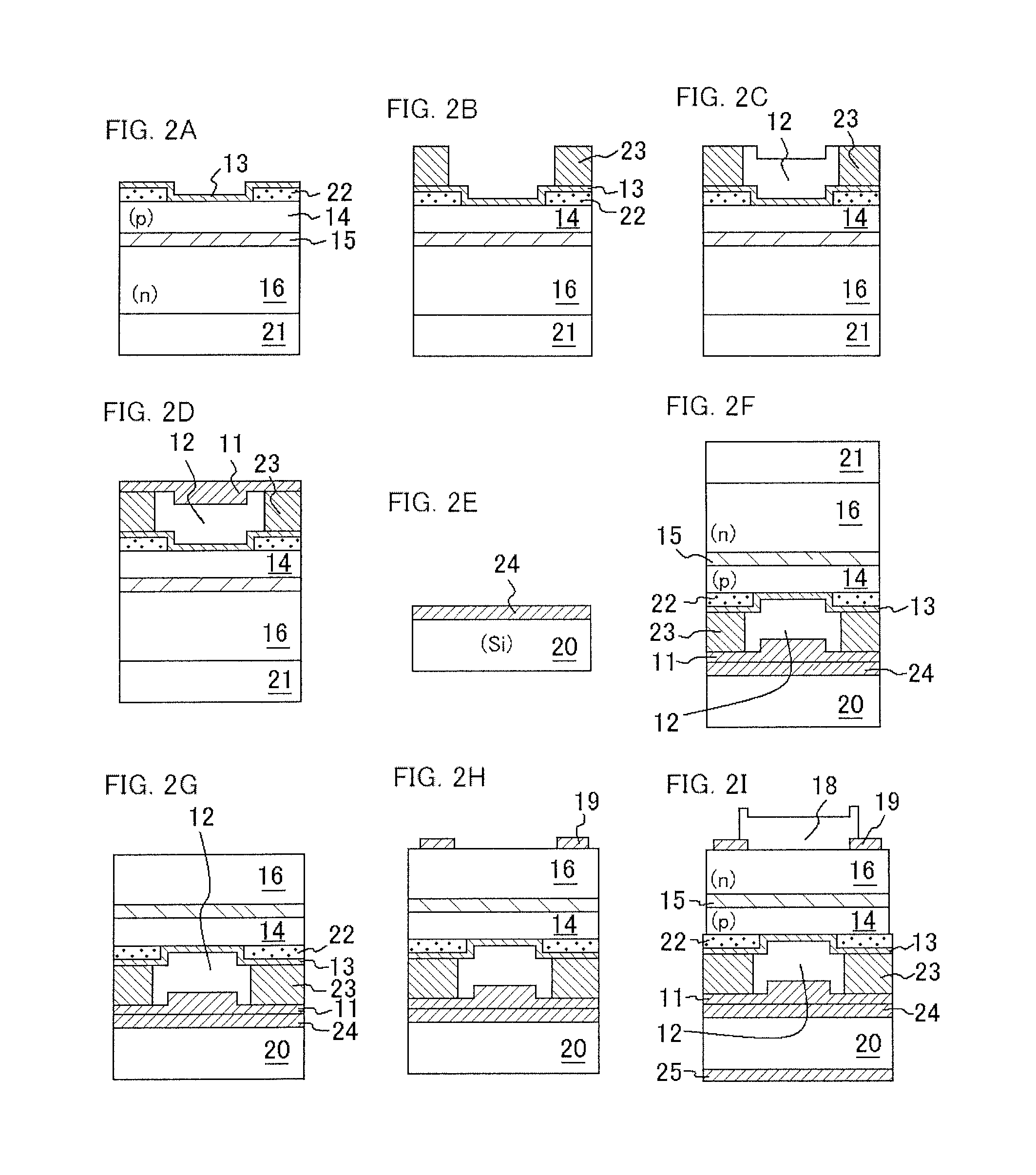
[0098]The nitride semiconductor light emitting element 100 of the present embodiment is constituted such that, as shown in FIG. 1, on the silicon substrate as the supporting substrate 20, a joining layer 24, a first electrode 11, a first Bragg reflector 12 made of a dielectric multilayer film, a first transparent electrode 13 made of ITO, a stacked layer body 17 of a nitride semiconductor, and a second Bragg reflector 18 made of a dielectric multilayer film, stacked in this order. Also, a connecting electrode 23 which is electrically connected to both the first electrode 11 and the first transparent electrode is formed on a side surface of the first Bragg reflector 12.
[0099]Further, a second electrode 19 which is electrically connected to the upper surface of the stacked layer body 17 is formed in the periphery of the second Bragg reflector 18. An insulating layer 22 made of SiO2 is disposed in the periphery of the element and between the first transparent electrode 13 and the stack...
embodiment 2
[0124]As shown in FIG. 6, the nitride semiconductor light emitting element 200 of the present embodiment, the second transparent electrode 27 is disposed in the central portion over the second conductive-type layer 16 via the insulating layer 26. The second Bragg reflector 18 is formed right on the second transparent electrode 27. The structure of the nitride semiconductor light emitting element 200 is substantially the same as that in Embodiment 1 except the portions described above. With such a structure, in which the transparent electrodes are disposed to the both sides (over, or below or under) of the stacked layer body, in addition to the effect described in Embodiment 1, the electric current which tends to crowd at the periphery of the element region can be well dispersed into the central portion. Thus, lateral distribution of light and gain can be well matched and laser oscillation characteristics can be improved. The present embodiment is particularly advantageous particular...
embodiment 3
[0125]As shown in FIG. 7, the nitride semiconductor light emitting element 400 of the present embodiment has a stacked layer body 17 processed into a cylinder shape by etching the first conductive-type layer 14, the light emitting layer 15 and the second conductive-type layer 16 in the film thickness direction. Also, the entire side surface of the cylinder is covered with an insulating film 29 made of SiO2. The structure of the nitride semiconductor light emitting element 400 is substantially the same as that in Embodiment 1 except the portions described above. With such a structure, lateral light can be more strongly confined than in Embodiment 1.
PUM
 Abstract
Description
Claims
Application Information