

Semiconductor laser device
a laser device and semiconductor technology, applied in semiconductor lasers, laser details, electrical equipment, etc., can solve the problems of reducing light absorption, not being able to further reduce prior art techniques that are not adequate to achieve the effect of further reducing the power consumption of semiconductor laser devices, reducing power consumption, and high electrical-to-optical power conversion efficiency
- Summary
- Abstract
- Description
- Claims
- Application Information
AI Technical Summary
Benefits of technology
Problems solved by technology
Method used
Image

Examples
first embodiment
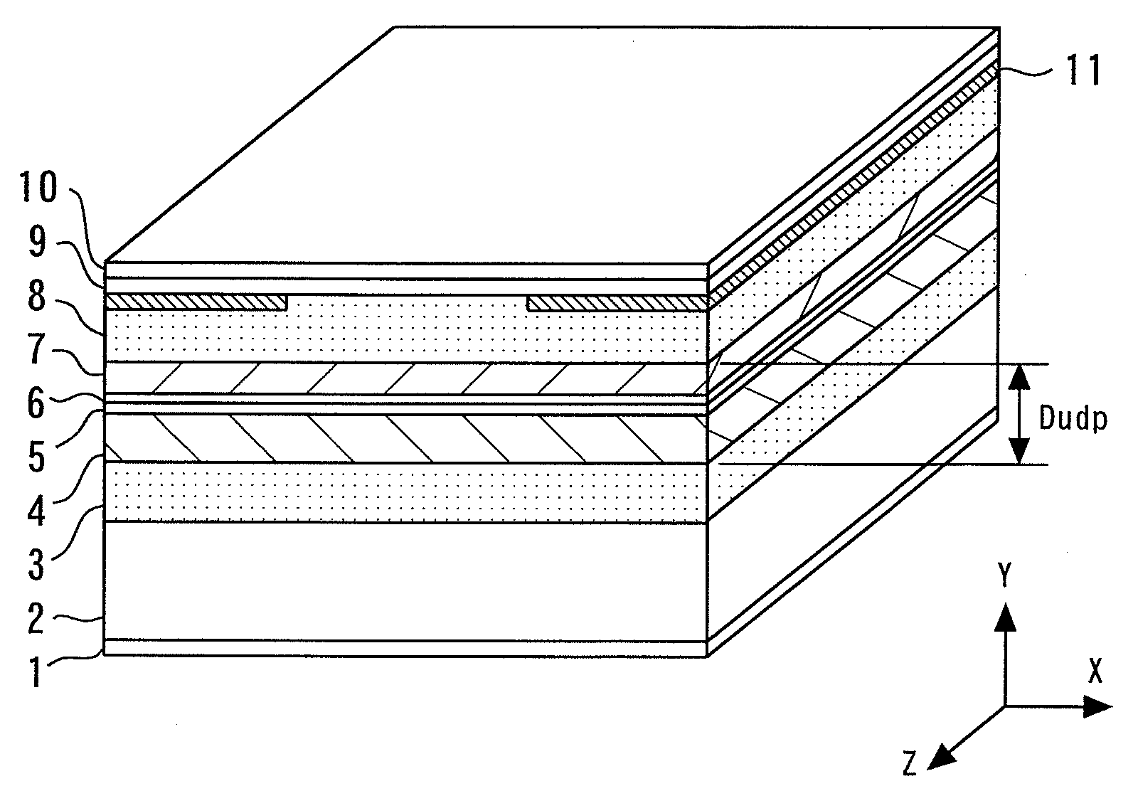
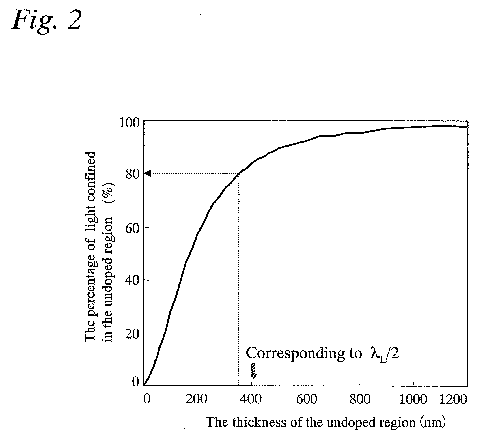
[0042]FIG. 1 is a perspective view of an 810 nm semiconductor laser device used to illustrate features of a first embodiment of the present invention. With reference to FIG. 1, the following describes the advantages obtained when the undoped region of the device, which includes the guiding and active layers, etc., has a thickness at least 0.5 times the oscillation or lasing wavelength.
[0043]The reference numerals and corresponding components in FIG. 1 are as follows: 1, an n-electrode; 2, an n-type GaAs substrate; 3, an n-type AlxGa1-xAs cladding layer with a thickness of 1.5 μm (where the Al mole fraction x=0.55); 101, an n-side AlyGa1-yAs outer guiding layer with a thickness of t / 2 nm (where y=0.35); 6, an AlwGa1-wAs active layer with a thickness of 10 nm (where w=0.10); 102, a p-side AlsGa1-sAs guiding layer with a thickness of t / 2 nm (where s=0.35); 8, a p-type AltGa1-tAs cladding layer with a thickness of 1.5 μm (where t=0.55); 9, a p-type GaAs contact layer; 10, a p-electrode;...
second embodiment
First Practical Example of Second Embodiment
[0078]FIG. 13 is a perspective view of an 810 nm semiconductor laser device according to a second embodiment of the present invention. Reference numerals and corresponding components in FIG. 13 are as follows: 62, an n-side AlyGa1-yAs guiding layer with a thickness of 700 nm (where y=0.35); and 63, a p-type AltGa1-tAs cladding layer with a thickness of 1.5 μm (where t=0.60). This semiconductor laser device is substantially similar to that of the first practical example of the first embodiment (shown in FIG. 3) except the configuration of an inner guiding layer.
[0079]Since the AlGaAs active layer 6 is located closer to the p-type AlGaAs cladding layer 63 than to the n-type AlGaAs cladding layer 3, fewer carriers are present within the guiding layers, as compared to when the active layer is spaced equally from the n-type and p-type cladding layers. This reduces the free carrier absorption and the resulting loss in the device, thereby increas...
third embodiment
First Practical Example of Third Embodiment
[0091]FIG. 20 is a perspective view of an 810 nm semiconductor laser device according to a third embodiment of the present invention. In FIG. 20, reference numeral 80 denotes a p-type AltGa1-tAs cladding layer with a thickness of 1.5 μm (where t=0.60). This semiconductor laser device is similar to that shown in FIG. 3, except that the p-type cladding layer 8 is replaced by the p-type AltGa1-tAs cladding layer 80. Since the AlGaAs active layer 6 is located closer to the p-type AlGaAs cladding layer 80 than to the n-type AlGaAs cladding layer 3, fewer carriers are present within the guiding layers, as compared to when the active layer is spaced equally from the n-type and p-type cladding layers. This reduces the free carrier absorption and the resulting loss in the device, thereby increasing the slope efficiency.
[0092]Further, the n-side inner guiding layer has a higher refractive index than the p-side guiding layer, by forming the n-side gui...
PUM
 Abstract
Description
Claims
Application Information