Method for manufacturing electronic device and method for manufacturing piezoelectric device

a piezoelectric device and electronic device technology, applied in piezoelectric/electrostrictive transducers, device material selection, solid-state diffusion coating, etc., can solve the problems of difficult crystal formation in consideration of vibration mode, inefficient use of piezoelectric materials, and limited material selection to aln or other suitable materials

Active Publication Date: 2010-05-06
MURATA MFG CO LTD
View PDF8 Cites 24 Cited by
  • Summary
  • Abstract
  • Description
  • Claims
  • Application Information

AI Technical Summary

Benefits of technology

[0015]To overcome the problems described above, preferred embodiments of the present invention provide a meth

Problems solved by technology

However, when the deposition method described above is used, the material is limited to AlN or other suitable material because of, for instance, the film formation temperature or the film formation conditions for obtaining a desired oriented film.
Furthermore, since the orientation direction of a crystal axis cannot be controlled, it is difficult to form a crystal in consideration of vibration mode.
When the polishing method described above is used, since the portion other than the piezoelectric thin film is treated as polishing waste, the piezoelectric material is not efficiently used.
In addition, it is difficult to form a piezoelectric thin film having a uniform thickness due to polishing conditions, variations in the shape of the original piezoelectric substrate, or other factors, which decreases productivity.
However, since the heating needs to be performed at a high temperature of about 450° C., the following problems arise.
As a result, its piezoelectr

Method used


Image

  • Method for manufacturing electronic device and method for manufacturing piezoelectric device
  • Method for manufacturing electronic device and method for manufacturing piezoelectric device
  • Method for manufacturing electronic device and method for manufacturing piezoelectric device

Examples


Embodiment Construction

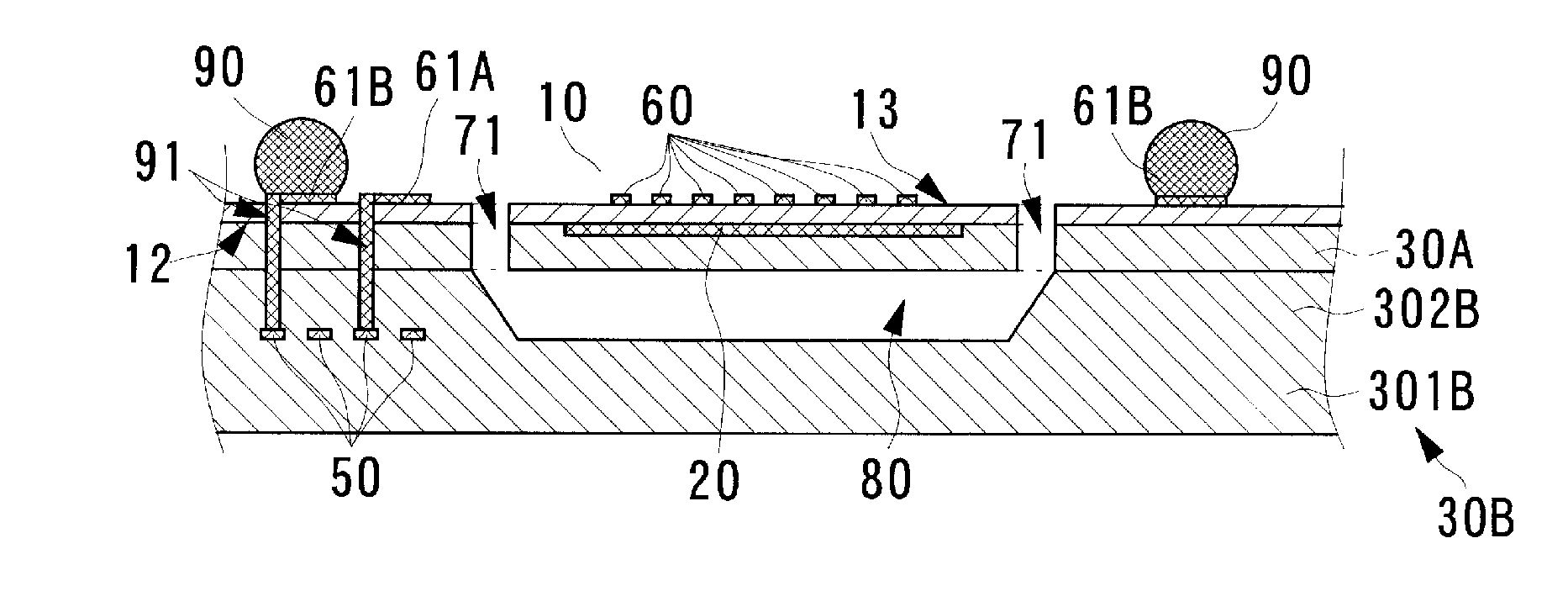
[0046]A method for manufacturing an electronic device according to preferred embodiments of the present invention will be described with reference to the drawings. In the following description, a thin film piezoelectric device for a Lamb wave that includes a piezoelectric thin film is described as an electronic device that uses a crystalline material.

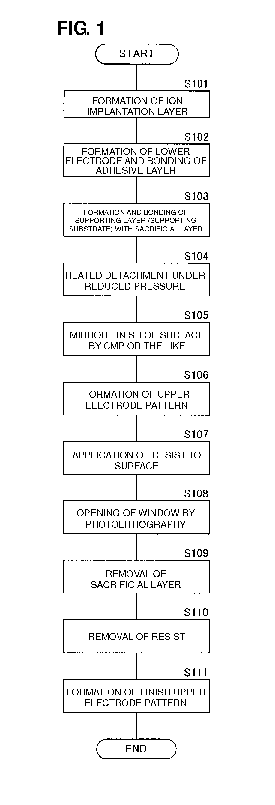
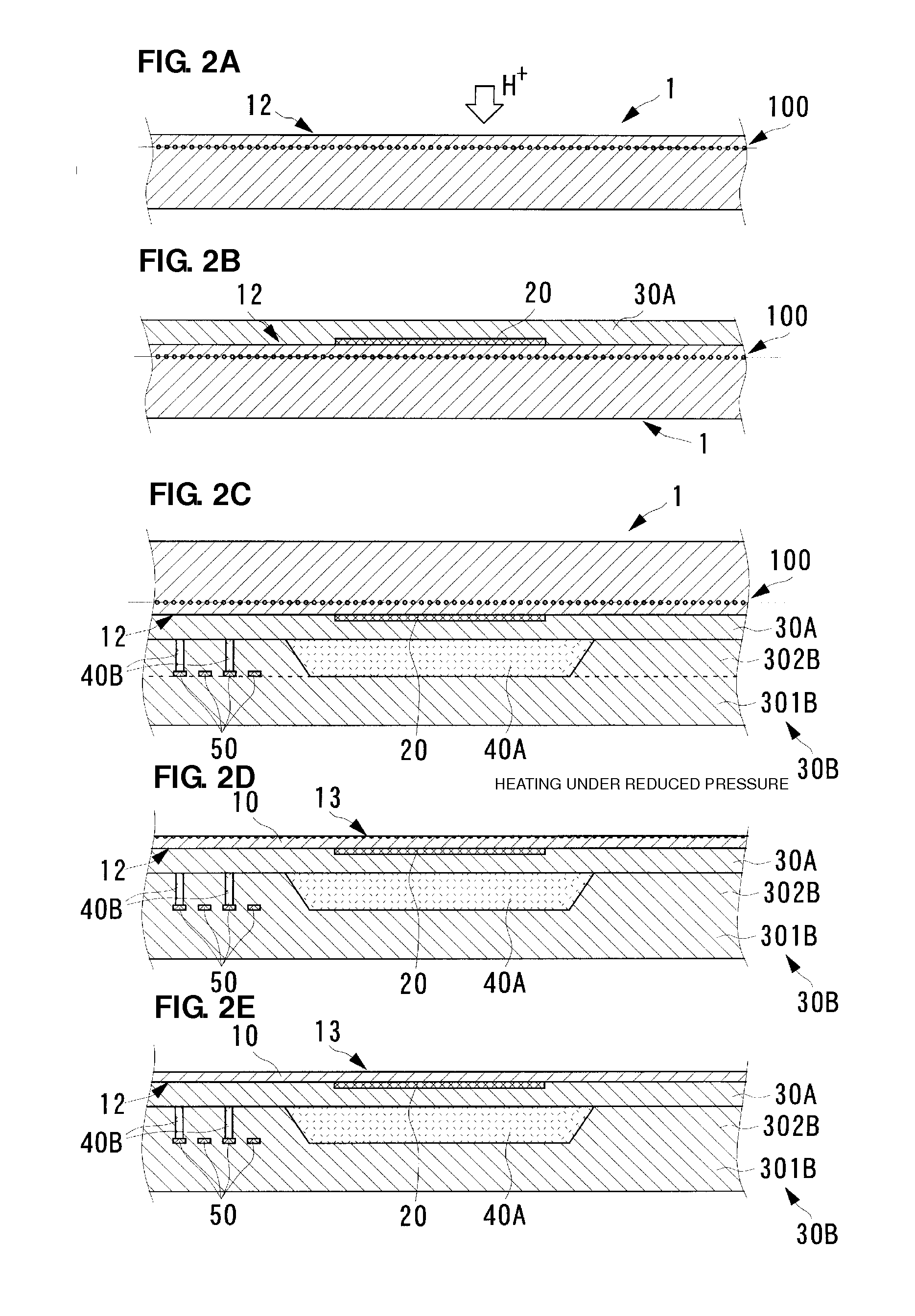
[0047]FIG. 1 is a flowchart showing a method for manufacturing a thin film piezoelectric device according to a preferred embodiment. FIGS. 2 to 4 schematically show the manufacturing processes of the thin film piezoelectric device formed in accordance with the manufacturing flow shown in FIG. 1.

[0048]A piezoelectric single crystal substrate 1 having a desired thickness is prepared. As shown in FIG. 2A, hydrogen ions are implanted from the back surface 12 side to form an ion implantation layer 100 (FIG. 1: S101). A mother substrate on which a plurality of separate thin film piezoelectric devices can be arranged is provided as the piezoel...


PUM

PropertyMeasurementUnit
Temperatureaaaaaaaaaa
Pressureaaaaaaaaaa
Adhesivityaaaaaaaaaa

Abstract

In a method for manufacturing an electronic device, an ion implantation layer is formed at a desired depth from one principal surface of a piezoelectric single crystal substrate by implanting hydrogen ions into the piezoelectric single crystal substrate under desired conditions. The piezoelectric single crystal substrate in which the ion implantation layer has been formed is bonded to a supporting substrate, and a piezoelectric thin film is then formed by the application of heat using the ion implantation layer as a detaching interface. This heated detachment is performed at a reduced pressure less than atmospheric pressure and at a heating temperature determined in accordance with the reduced pressure.

Description

BACKGROUND OF THE INVENTION[0001]1. Field of the Invention[0002]The present invention relates to a method for manufacturing an electronic device including a crystalline material, and particularly to a method for manufacturing a thin film piezoelectric single crystal device.[0003]2. Description of the Related Art[0004]Various electronic devices, such as semiconductors and piezoelectric bodies, that include a crystalline material having certain electrical characteristics are currently manufactured and used. Among the various electronic devices, a surface acoustic wave (SAW) device, a film bulk acoustic resonator (F-BAR) device, and other devices are exemplified as a piezoelectric device. Furthermore, many thin film piezoelectric devices obtained by reducing the thickness of a piezoelectric body have been developed as the piezoelectric device because they support high-frequency Lamb wave devices. A method for manufacturing a piezoelectric thin film for forming such a thin film piezoele...

Claims


Application Information

Patent Timeline
IPC IPC(8): H01L41/22H01L41/09H01L41/18H01L41/312H03H3/08H03H9/25
CPCH03H3/02H01L41/313Y10T29/49147H03H2003/022H01L41/0933H03H2003/023H01L41/0973H01L41/1138Y10T29/49126H03H2003/021C23C8/04H01L41/319Y10T29/49005C23C8/24H01L41/293Y10T29/49155Y10T29/42H10N30/073H10N30/079H10N30/308H10N30/2041H10N30/2047H10N30/063
Inventor IWAMOTO, TAKASHI
Owner MURATA MFG CO LTD
Why Eureka
Try Eureka