
Silicon carbide semiconductor device

a silicon carbide and semiconductor technology, applied in the direction of semiconductor devices, electrical devices, transistors, etc., can solve the problems of local overheating and destruction of devices, limit the safe operation of si pn diodes and in the si bjts, etc., and achieve small series resistance and wide safe operating area

Active Publication Date: 2010-05-13
SEMICON COMPONENTS IND LLC
View PDF19 Cites 16 Cited by
  • Summary
  • Abstract
  • Description
  • Claims
  • Application Information

AI Technical Summary

Benefits of technology

[0047]The advantages of a semiconductor device according to the present invention are a wider safe operating area under the following conditions: reverse recovery to high voltages with high dl/dt for SiC pn diodes, avalanche breakdown with high

Problems solved by technology

486, (2003)], and that a similar type of space charge effects limit the safe operating of Si pn diodes and in the Si BJTs.
At some critical combination of applied voltage and current density, the current controlled space charge will induce a negative differential resistance for the device, and this negative differential resistance leads to the formation of high current density filaments, which in most cases cause local overheating and destruction of the device.

Method used


Image

  • Silicon carbide semiconductor device
  • Silicon carbide semiconductor device
  • Silicon carbide semiconductor device

Examples


Embodiment Construction

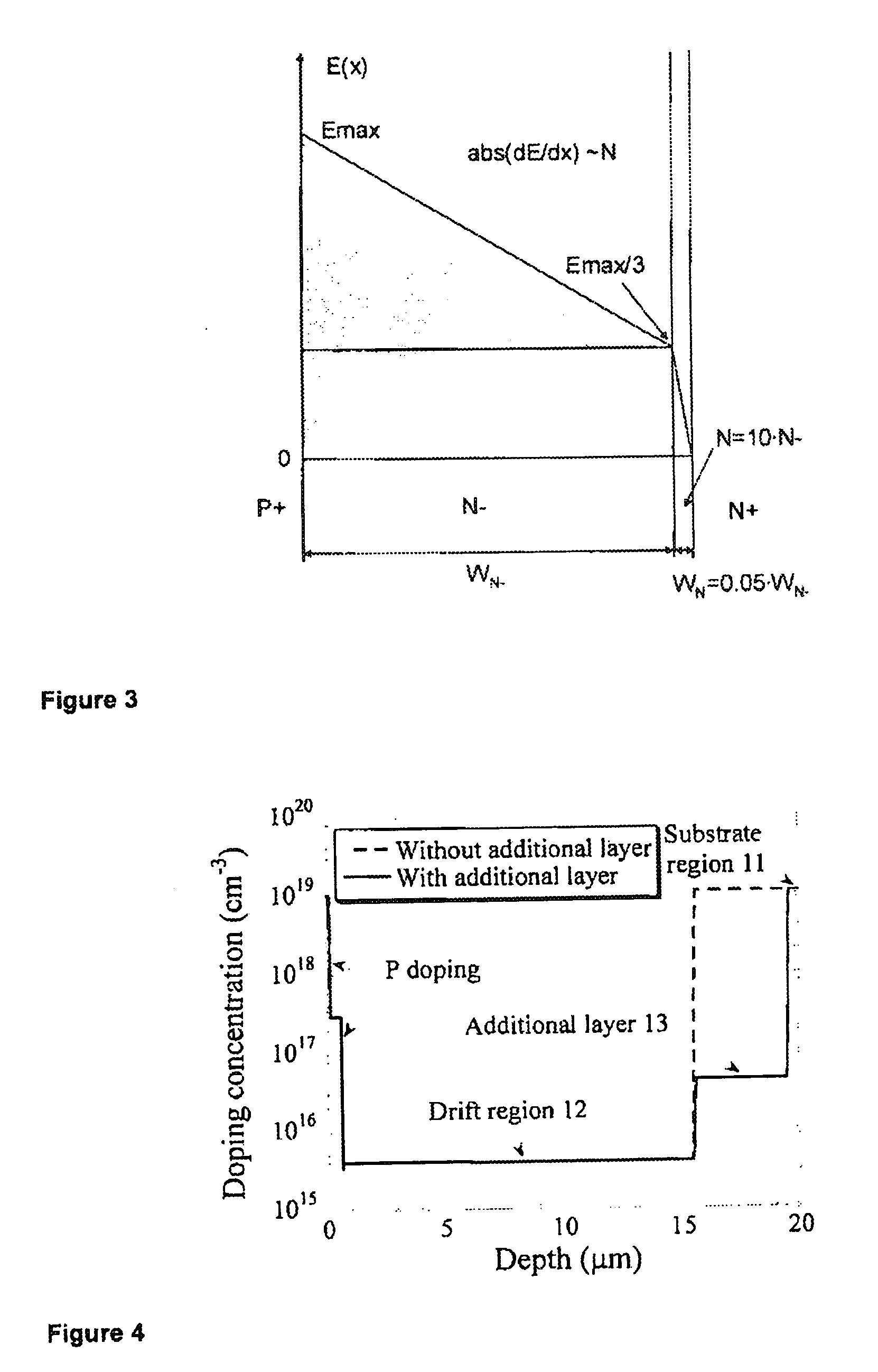
[0057]The present invention will now be described with reference to FIG. 4, where a silicon carbide bipolar junction transistor for power electronics applications, is described as an exemplifying embodiment of the invention.

[0058]FIG. 4 shows schematically a semiconductor device 1 in silicon carbide, with a highly doped substrate region 11 and a drift region 12.

[0059]An additional layer 13 is positioned between the highly doped substrate region 11 and the drift region 12, the additional layer 13 providing a wider safe operating area at high voltages with subsequently high current densities.

[0060]The additional layer 13 has the same type of doping as the substrate region 11 and the drift region 12, and the doping concentration in the additional layer 13 is higher than the doping concentration in the drift region 12 and lower than the doping concentration in the substrate region 11.

[0061]The presentment invention teaches that doping concentration of the additional layer 13 can be smal...


PUM


Abstract

The present invention relates to a semiconductor device (1) in silicon carbide, with a highly doped substrate region (11) and a drift region (12). The present invention specifically teaches that an additional layer (13) is positioned between the highly doped substrate region (11) and the drift region (12), the additional layer (13) thus providing a wide safe operating area at subsequently high voltages and current densities.

Description

FIELD OF INVENTION[0001]The present invention relates to a semiconductor device in silicon carbide, with a highly doped substrate region and a drift region.DESCRIPTION OF BACKGROUND ART[0002]Silicon carbide (SiC) has excellent properties for fabrication of power semiconductor devices. SiC has due to its wide bandgap nearly ten times higher critical field strength than silicon and the wide bandgap also provides the possibility for devices that can operate at high temperatures. The thermal conductivity of SiC is also 2-3 times higher than for Si and this improved heat transport means that SiC devices can operate at higher power densities without being overheated.[0003]Power switching transistors and diodes are used in a wide variety of power electronic systems such as power supplies, motor drives, welding, electric vehicles, trains and transmission and distribution of electric power on the grid[0004]It is important to reduce power losses in power transistors and diodes as much as poss...

Claims


Application Information

Patent Timeline
IPC IPC(8): H01L29/24
CPCH01L29/0615H01L29/0821H01L29/1608H01L29/36H01L29/66068H01L29/868H01L29/73H01L29/0611H01L29/732H01L29/7371
Inventor DOMEIJ, MARTIN
Owner SEMICON COMPONENTS IND LLC
Learn More