Semiconductor device and capacitance regulation circuit

a capacitance regulation circuit and semiconductor technology, applied in the field of semiconductor devices and capacitance regulation circuits, can solve the problems of destroying the insulated gate semiconductor chip, the gate of the igbt, and the high current change rate (di/dt), and achieves low noise, wide safe operation area, and low loss

Inactive Publication Date: 2006-11-28
KK TOSHIBA
View PDF18 Cites 7 Cited by
  • Summary
  • Abstract
  • Description
  • Claims
  • Application Information

AI Technical Summary

Benefits of technology

[0029]According to the invention, dI / dt at the switching and the surge voltage resulting from it can be suppressed, and the insulated control semiconductor device having a low noise, low loss, and a wide safe operating area can be offered.
[0030]In particular, according to the first embodiment, since a capacitor is made to add at inside or near the semiconductor element, the reliability as a capacitor becomes high and thus, the insulated control semiconductor device which can prevent malfunction certainly even in the large-sized multi-chip type form can be offered.
[0031]Moreover, according to the second embodiment, it becomes possible to add a capacitor to a switching element with the optimal timing and the optimal period, and switching time is not increased unnecessarily. Rather, since the control resistance can be made smaller than before, switching time becomes shortened and loss can also be reduced. That is, the insulated control semiconductor device and a capacitance regulation circuit which can realize the low noise characteristics by suppression of dI / dt at switching and by suppression of the surge voltage resulting from it, shortening of the switching time and low loss can be offered.
[0032]As a result, total loss becomes lower than before, stable operation can be enabled and thus the merit on industry is great.

Problems solved by technology

However, these measures produce a high rate of voltage change (dV / dt) and a high rate of current change (dI / dt).
As a result, the insulated gate semiconductor device may have a bad influence on peripheral equipment by emitting a noise out of the device, or malfunction may arise because device's own gate voltage is changed.
Furthermore, an excessive surge voltage may also cause the destruction of insulated gate semiconductor chip and / or a free wheeling diode (FWD) chip connected in parallel to the insulated gate semiconductor chip.
Particularly, although when the insulated gate semiconductor chip is turned on the FWD which is connected to the turned on chip in series and forms the arm of a bridge circuit will carry out reverse recovery operation, when dV / dt of FWD becomes high there becomes a danger that the gate of the IGBT which is connected in parallel to the FWD and should be in the OFF state may be charged and malfunction (turning into ON state) may occur.
Particularly, when excessive dI / dt and dV / dt occur, a large electric power arises momentarily in FWD and the problem that FWD may breaks occurs.
That is, since the problems that Err of FWD increases and that FWD breaks occurred, there was a limit in making the switching speed higher, and consequently, there was a limit in reducing the total loss of the power converter.
However, it was difficult to stably suppress the change of Vge of the insulated gate semiconductor chip itself by such conventional techniques, because of the impedance inside the semiconductor device, the impedance up to the connection point of the capacitor CGE connected at the exterior of the semiconductor device, and the inductance of the CGE itself.
Especially, in the large-sized package for the large current capacity which includes many insulated gate semiconductor chips, since the gate wiring in a package becomes long, the parasitic inductance cannot be disregarded.
As a result, it was difficult to stably suppress the changes in Vge for every chip with the conventional structure.
Moreover, connecting the capacitor outside the device had the problem of not being mechanically reliable.
That is, since the generation of heat from the insulated gate semiconductor chip is relatively large, if capacitor CGE is mounted on the same mounting substrate as the insulated gate semiconductor chip, the influence of the rise of temperature cannot be disregarded.
As a result, there is a possibility that the thermal fatigue of solder which mounts capacitor CGE may arise.
Moreover, since there is “variation” in a temperature coefficient for each capacitor CGE, there is a possibility that the switching operation of two or more chips provided in the same equipment becomes less uniform.
Furthermore, if the insulated gate semiconductor chips which serve as a heat source are separated from the capacitors CGE in order to prevent these problems, it becomes necessary to enlarge the mounting substrate, and as a result, the size of the semiconductor device becomes enlarged.
As mentioned above, when gate resistance is reduced for the reduction of loss in the conventional insulated gate semiconductor device, high dI / dt, high dV / dt, and a high surge voltage may occur, IGBT / FWD may be broken, the noise may be emitted to the environment, and malfunction may be carried out by its own change of Vge.
Moreover, there was a limit in reduction of total loss including IGBT and FWD.
Furthermore, since the impedance from each chip was not able to be disregarded in a large-sized insulated gate semiconductor device by the method of connecting the external capacitor CGE to the exterior of the semiconductor device, it was difficult to stably suppress change in Vge of the semiconductor chips.
Furthermore, when the capacitors CGE are incorporated on the same mounting substrate as the insulated gate semiconductor chips, there is concern about the influence by heat.

Method used


Image

  • Semiconductor device and capacitance regulation circuit
  • Semiconductor device and capacitance regulation circuit
  • Semiconductor device and capacitance regulation circuit

Examples


first embodiment

[0068](First Embodiment)

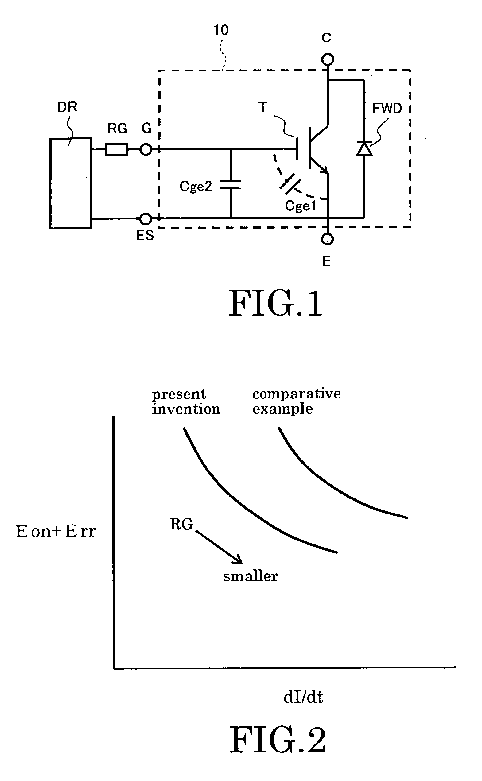
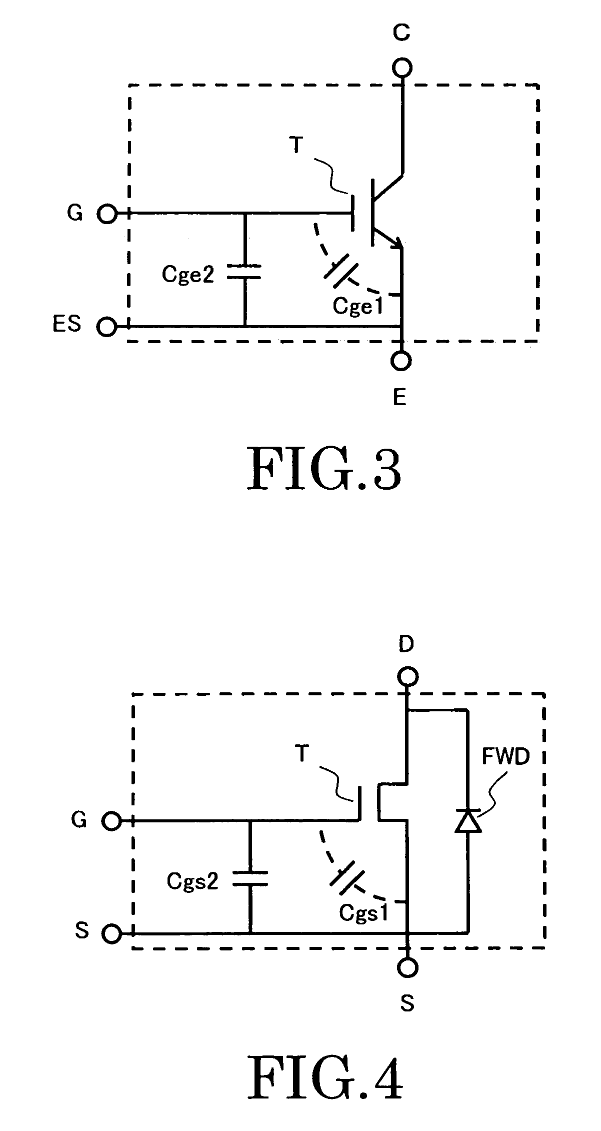
[0069]First, a semiconductor device integrated with a capacitor Cge2 which adjusts the capacitance between the gate and the emitter of an insulated gate semiconductor chip will be explained as a first embodiment of the invention, referring to FIG. 1 through FIG. 17.

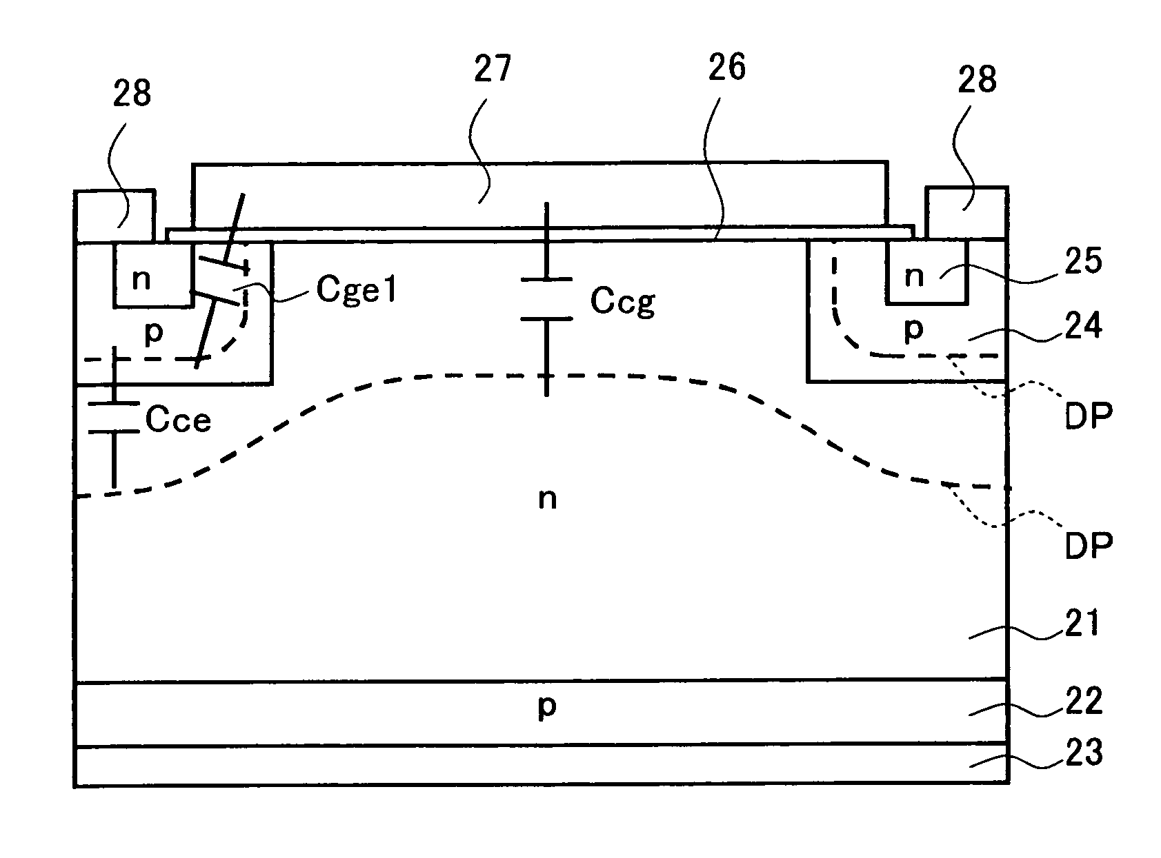
[0070]FIG. 1 is a schematic diagram illustrating the insulated gate semiconductor device and the drive circuit connected thereto according to the first embodiment of the invention. That is, the semiconductor device 10 shown in this figure is an insulated gate semiconductor device including the switching chip T and a FWD chip. The switching chip T and FWD are connected in parallel and in opposite directions. As a switching chip T, IGBT or various kinds of insulated gate semiconductor chips can be used as will be explained detail after.

[0071]This semiconductor device 10 has the collector terminal C as a first main electrode, the emitter terminal E as a second main electrode, and gate terminal G as a ...

second embodiment

[0136](Second Embodiment)

[0137]Next, the semiconductor device which includes a capacitance regulation circuit which add a given capacitor between the gate and the emitter only in the partial period of the switching will be explained as a second embodiment of the invention.

[0138]FIG. 18 is a conceptual diagram showing the fundamental structure of the embodiment. That is, the insulated gate switching element T has the collector main electrode C, the emitter main electrode E, and the gate electrode G. As the switching element, various kinds of elements which have the insulated gate structure, such as IGBT and Power MOS, for example, can be used.

[0139]The parasitic capacitance Cge between the gate and the emitter, and the parasitic capacitance Cgc between the gate and the collectors exist inside of the switching element T. And gate voltage Vgg is applied appropriately between the gate control electrode G and the emitter sense electrode ES, and thus, the switching operation is controlled...


PUM


Abstract

According to an embodiment of the invention, there is provided a semiconductor device comprising: a semiconductor element having a first main electrode, a second main electrode and a control electrode, a current flowing between the first and second main electrodes being controlled by a control signal which is input between the control electrode and the second main electrode; and a capacitor formed by providing an insulating layer between the second main electrode and the control electrode of the semiconductor element.

Description

CROSS-REFERENCE TO RELATED APPLICATIONS[0001]This application is based upon and claims the benefit of priority from the prior Japanese Patent Application No. 2002-161469, filed on Jun. 3, 2002; the entire contents of which are incorporated herein by reference.BACKGROUND OF THE INVENTION[0002]The present invention relates to a semiconductor device and a capacitance regulation circuit, and more particularly, to a insulated gate semiconductor device such as MOSFET (Metal-Oxide-Semiconductor Field Effect Transistor), insulated gate bipolar transistor (IGBT), and injection enhanced gate transistor (IEGT), and to a capacitance regulation circuit which adjusts the capacitance of these semiconductor devices dynamically.[0003]In order to use electric energy effectively, power converters, such as an inverter, are used widely. And as a semiconductor device for electric power control used for these power converters, the insulated gate semiconductor devices which have an excellent controllabilit...

Claims


Application Information

Patent Timeline
Patent Type & Authority Patents(United States)
IPC IPC(8): H01L29/43H01L23/498H01L25/07H01L27/04H01L27/07H01L29/423H01L29/739H01L29/78
CPCH01L23/49844H01L23/642H01L25/072H01L25/16H01L25/162H01L27/0727H01L29/402H01L29/407H01L29/7395H01L29/7397H01L29/7803H01L29/7813H03K17/04123H03K17/042H03K17/0814H03K17/12H03K17/162H03K17/168H03K17/567H03K17/687H01L2924/1305H01L2924/1301H01L2924/01055H01L2924/01021H01L24/49H01L2224/48091H01L2224/49111H01L2924/13055H01L2924/13091H01L2924/19041H01L2924/19105H01L2924/30107H01L2924/3011H03K2217/0036H01L24/48H01L2924/00014H01L2924/00H01L2224/05599H01L2224/45099H01L2224/85399H01L2224/0603H01L2224/45015H01L2924/207
Inventor SUGIYAMA, KOICHIINOUE, TOMOKI
Owner KK TOSHIBA
Why Eureka
Try Eureka