Magnetic Data Storage Device and Method

Inactive Publication Date: 2010-05-20
INGENIA HLDG LTD
View PDF13 Cites 113 Cited by
  • Summary
  • Abstract
  • Description
  • Claims
  • Application Information

AI Technical Summary

Benefits of technology

[0016]The direction of propagation of the domain walls along the nanowire depends on the direction of rotation of the magnetic field. Thus, it is possible to select at which end of the nanowire the data is read out. For a first-in first-out shift register, each data read-out element is arranged at the opposite end of its associated nanowire to the data input element. The domain walls are propagated right along the nanowire from the first end to the other. Conversely, for a first-in last-out shift register, each data read-out element is ar

Problems solved by technology

In this manner, a known problem with domain wall propagation in nanowires, whereby an externally applied magnetic field aligned along the le

Method used


Image

  • Magnetic Data Storage Device and Method
  • Magnetic Data Storage Device and Method
  • Magnetic Data Storage Device and Method

Examples


example 1

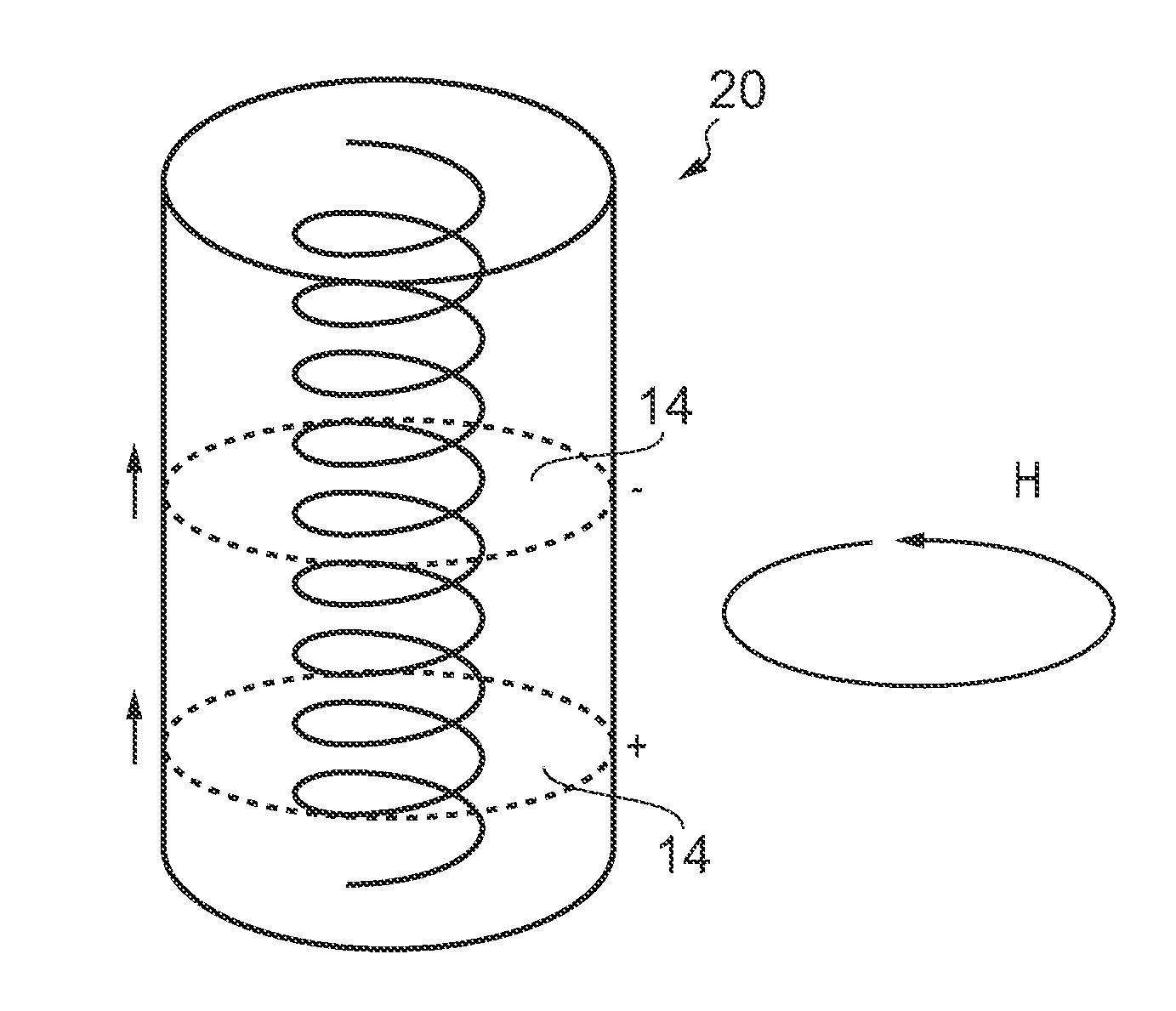
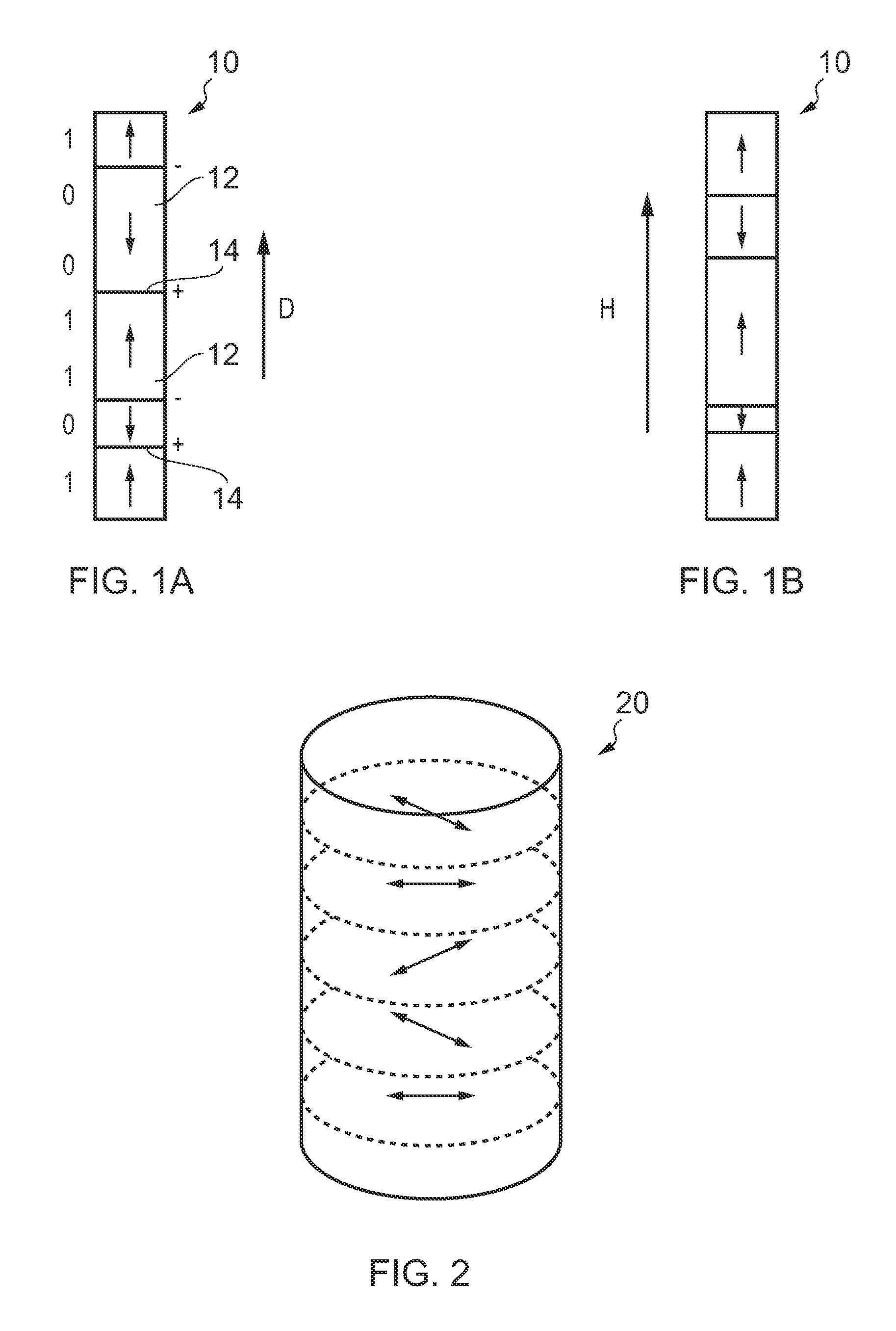
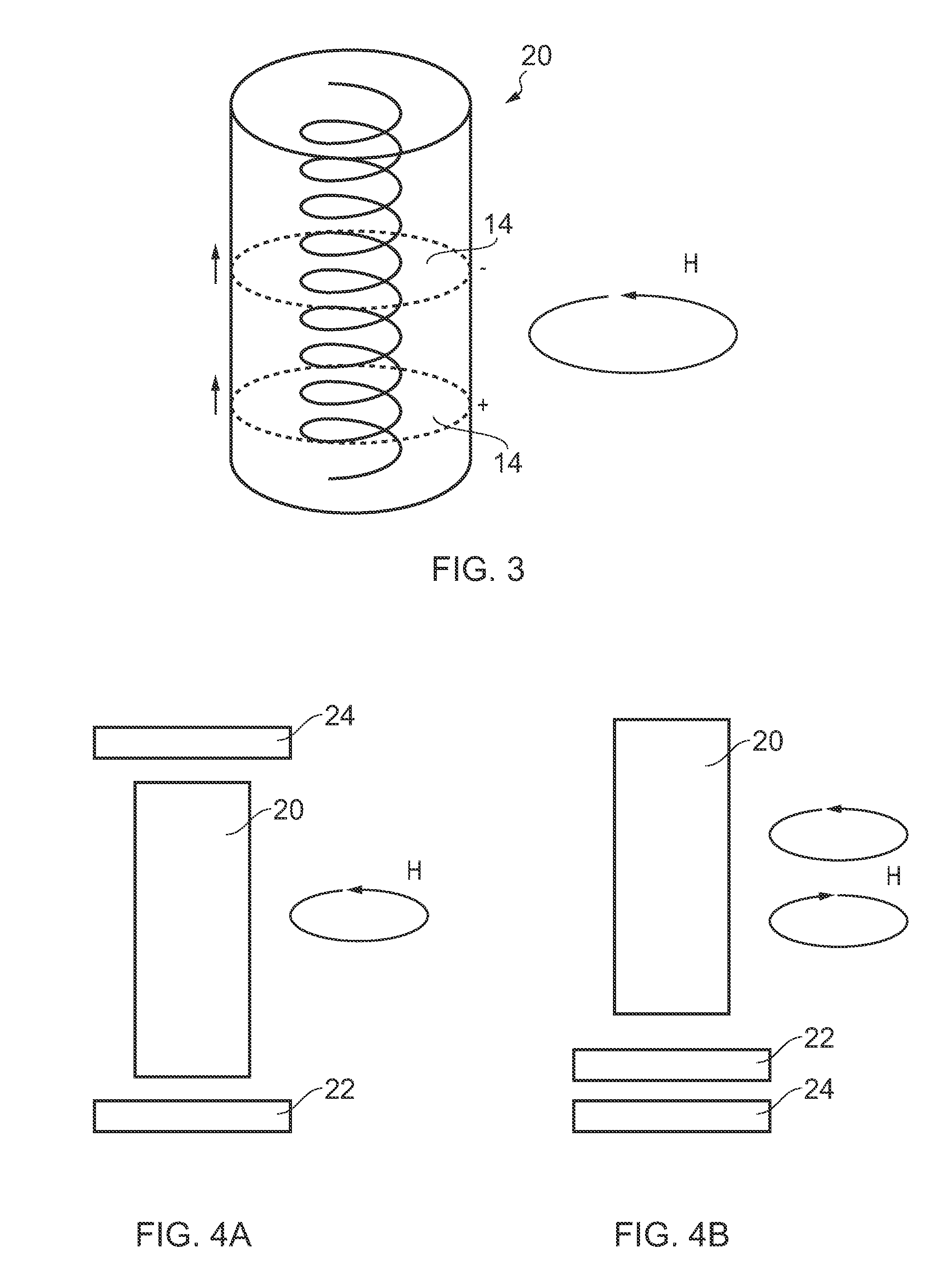
[0076]300 nm diameter pillars arranged on a substrate in a 350 nm square pitch. Each pillar is 3 μm high, and the pitch of the anisotropy spiral is 100 nm. These dimensions represent conservative values for the capability for lithography (current state of the art lithography resolution being 45 nm). The spiral pitch is selected so that it is not less than the width of a domain wall for the anisotropy of the magnetic material (so that the domain walls are properly separated for correct propagation along the spiral by the rotating magnetic field); in this example the pitch is approximately equal to the wall width, although a bigger pitch may be optimum. These values give an effective areal density of 160 Gbits / inch2, which is 16 times higher than the current state of the art for Flash memory even though the selected values are conservative.

example 2

[0077]Magnetic material in anodic aluminium oxide pores, the pores on a 200 nm square pitch. However, to avoid any alignment difficulties, the data input and read-out elements are 1 μm2, so that each addresses multiple nanowires (thereby reducing the data density). The pores are 1 mm in height, and the pitch of the anisotropy spiral is 50 nm. This gives an effective areal density of 13,000 Gbits / inch2, vastly superior to the state of the art for either hard disk drives or Flash memory.

[0078]Thus, it can be seen that the present invention offers great potential for offering improvements in data storage.

[0079]The term “nanowire” is used throughout this specification and the appended claims. However, it is not intended that the invention be limited to structures of magnetic material with dimensions that strictly comply with this term. Any magnetic material structure having dimensions that allow formation and propagation of domain walls in the described manner is intended to be included...


PUM


Abstract

A data storage device comprises an array of parallel magnetic nanowires each having a uniaxial anisotropy with an easy axis substantially perpendicular to the longitudinal axis of the nanowire and which is rotated about the longitudinal axis along the length of the nanowire, and a magnetisation state that follows the easy axis, where each nanowire has a data input element for nucleating magnetic domains separated by domain walls in an end of the nanowire, the sequence of domains and walls representing binary data, and a data read-out element operable to detect the magnetisation at an end of the nanowire, the device also comprising a magnetic field source operable to generate a magnetic field rotating in a plane substantially perpendicular to the longitudinal axes of the nanowires so as to propagate domain walls along the at least one nanowire. Reversal of the direction of rotation of the magnetic field reverses the propagation direction of the domain walls, so that data can be moved in either direction along the nanowires.

Description

BACKGROUND OF THE INVENTION[0001]The present invention relates to a magnetic data storage device and a method for storing data using magnetic nanowires.[0002]Current data storage devices for storing data files (contiguous blocks of data) are typically either hard disk drives or non-volatile semiconductor memory such as Flash memory. Non-volatile semiconductor devices are attractive because they are compact and fast, and unlike hard disk drives, have no moving parts. However, the cost-per-bit for semiconductor storage is presently about 100 times higher than for hard disk storage, making the latter still popular. A major advance in the speed and portability of data storage could occur if a non-volatile solid-state memory (hence having no moving parts) could be fabricated with 10 to 100 times the storage density of current solid-state devices but at the same cost. This combination of features would allow hard disk storage to be replaced by solid-state storage.[0003]The currently known...

Claims


Application Information

Patent Timeline
IPC IPC(8): G11C19/00H01L21/00
CPCB82Y10/00G11C19/0816G11C11/155G11C11/14G11C11/12G11C11/5607
Inventor COWBURN, RUSSELL PAUL
Owner INGENIA HLDG LTD
Why Eureka
Try Eureka