Solder ball

a technology of solder balls and solder balls, which is applied in the field of solder balls, can solve the problems of reduced yield, difficulty in completely preventing mounting errors, and limited organic compounds that cannot prevent the change in color sufficiently, so as to prevent the micro-bonding of solder balls, prevent the change in color of solder balls, and improve the yield of electronic devices

Inactive Publication Date: 2010-05-27
HITACHI METALS LTD
View PDF10 Cites 19 Cited by
  • Summary
  • Abstract
  • Description
  • Claims
  • Application Information

AI Technical Summary

Benefits of technology

[0018]The present invention can prevent the micro-bonding of the solder balls due to the triboelectric charging thereof, and prevent the change in color of the solder balls due to the oxidation of the surface of the solder ball, thereby improving the yield of the electronic devices in the ball mounting process. Additionally, the oxide film on the surface of the solder ball is reduced, which can improve the reliability of bonding between the solder balls.
[0019]The present invention can prevent the excessively adhesion of the solder balls to the ball mounting jig.
[0020]The present invention can prevent the malfunction of a device for detection of the mounted solder balls, and thus can improve the yield of the electronic devices.

Problems solved by technology

In such a ball mount process, the balls to be mounted may be micro-bonded together and not sucked by the mounting jig, or the balls may be attached to the mounting jig at the same time to cause a defective condition or the like.
The progress of oxidation of the solder ball, and of the etiolation of the surface may disadvantageously cause malfunction of the optical detector for detection of the mounted balls, which results in a decrease in yield.
The surface treatment using such kinds of limited organic compounds cannot sufficiently prevent the change in color of the solder balls, and has difficulty in completely preventing mounting errors from being caused by the micro-bonding between the solder balls due to the triboelectric charging as described above.
Further, in order to achieve mounting at high density, a pitch of electrodes on a substrate has become fine, and the diameter of a solder ball has decreased, which may cause problems, including micro-bonding and the like.
From the viewpoint of background described above, it is difficult for the related art to address the foregoing problems.
A high reflow temperature promotes the oxidation of the solder balls to reduce the wettability, which causes the problems associated with the reliability of bonding.

Method used


Image

  • Solder ball
  • Solder ball

Examples


examples 1 to 9

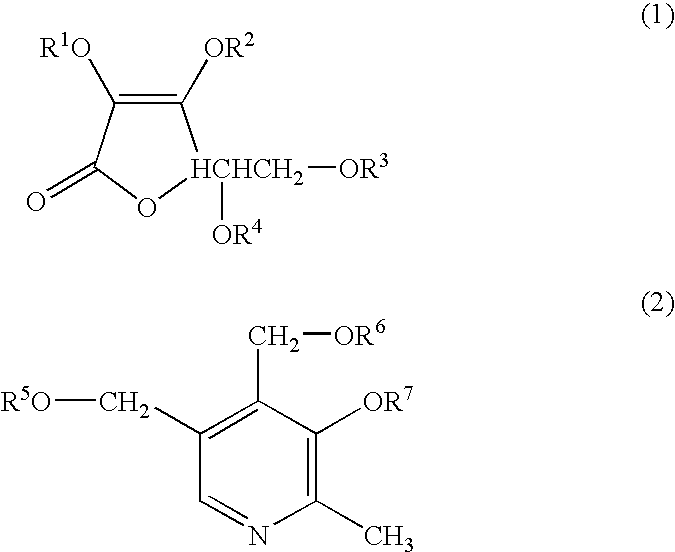
[0042]In Examples 1 to 9, the surface treatment was applied to solder balls made of Sn-3.0Ag-0.5Cu and having a grain size of 450 μm, and the flowability of the solder balls was evaluated. The surface treatment agents used were sorbitan monolaurate, sorbitan monopalmitate, sorbitan monostearate, sorbitan tristearate, sorbitan trioleate, retinol, tocopherol, pyridoxic acid dipalmitate and ascorbic acid dipalmitate, respectively. In order to coat the solder balls at a rate of 4.4 mg / m2, the surface treatment agent was dissolved in 2-propanol to produce a treatment solution.

[0043]Then, 10 g of the solder balls were sufficiently immersed in 0.8 g of the treatment solution added, and dried in a drying machine at 100° C. (degree C.) for 10 minutes, whereby the solder balls were coated with the surface treatment agent.

[0044]The friction between the thus-obtained solder balls was evaluated with reference to a flowability test method defined by JIS Z 2505. Metal funnels with different orific...

examples 10 to 15

[0049]In Examples 10 to 15, solder balls made of Sn-3.0Ag-0.5Cu and having grain sizes of 30 μm, 70 μm, 250 μm, 300 μm, 450 μm and 1000 μm were subjected to surface treatment, and then the flowability of the solder balls was evaluated. Pyridoxic acid dipalmitate which effectively worked in Example 8 was used as the surface treatment agent. The solder ball was coated with the surface treatment agent at a rate of 4.4 mg / m2 by the above-mentioned method. Evaluation of the flowability of the solder balls was performed by changing the orifice diameter of the funnel and the amount of sampling according to the grain size of the solder ball. The flowing times of the solder balls were measured on the following conditions. For the solder balls of 30 μm in grain size, the orifice diameter of the funnel was 0.2 mm, and the amount of sampling was 0.25 g. For the solder balls of 70 μm in grain size, the orifice diameter of the funnel was 0.3 mm, and the amount of sampling was 0.5 g. For the solde...

examples 16 to 25

[0054]In Examples 16 to 25, solder balls made of Sn-3.0Ag-0.5Cu and having a grain size of 450 μm were subjected to the surface treatment, and the flowability of the solder balls was evaluated. The surface treatment agents in use were pyridoxine monocaprylate, pyridoxine dicaprylate, pyridoxic acid monopalmitate and pyridoxic acid dipalmitate which were vitamin B6 derivatives, and ascorbic acid monopalmitate, ascorbic acid dipalmitate, ascorbic acid monostearate, ascorbic acid distearate, ascorbic acid tetraisopalmitate and ascorbyl tetra-hexyldecanoate which were vitamin C derivative. The solder balls were coated with the surface treatment agents at a rate of 4.4 mg / m2. The flowing times of the solder balls subjected to the above surface treatment were measured in the same way as Example 1.

[0055]Table 3 shows the results of Examples 16 to 25. As can be seen from Table 3, the solder balls of the present invention shown in Examples 16 to 25 have improved flowability by coating the so...


PUM

PropertyMeasurementUnit
grain sizeaaaaaaaaaa
thicknessaaaaaaaaaa

Abstract

An object of the present invention is to improve a yield of electronic devices in a ball mounting process by preventing a micro-bonding and change in color of the solder balls, and to improve a bonding reliability of the solder balls by reducing an oxide film on a surface of the solder ball.The solder ball has a surface thereof coated with an organic compound containing a cyclic structure and an aliphatic hydrocarbon group.

Description

CLAIM OF PRIORITY[0001]The present application claims priority from Japanese patent application serial No. 2008-294066, filed on Nov. 18, 2008, the content of which is hereby incorporated by reference into this application.BACKGROUND OF THE INVENTION[0002]1. Field of the Invention[0003]The present invention relates to solder balls.[0004]2. Description of Related Art[0005]In recent years, electronic devices have increased in communication speed and capacity, and become multifunctional and portable at a rapid pace. The advance of surface mount technology (ball grid array (BGA) / chip scale package (CSP)) of a package for a semiconductor integrated circuit or the like has improved fine wiring and multiple pins, thus leading to increase in communication speed and portability.[0006]Unlike conventional bonding methods using a metal lead frame, such as a quad flat package (QFP) or a small outline package (SOP), the BGA / CSP technology involves forming bumps using solder balls, and then direct...

Claims


Application Information

Patent Timeline
Patent Type & Authority Applications(United States)
IPC IPC(8): B23K35/14B23K35/22
CPCB23K35/22H05K3/3478B23K35/365B23K35/226
Inventor OTA, RYOITABASHI, TAKEYUKI
Owner HITACHI METALS LTD
Why Eureka
Try Eureka