

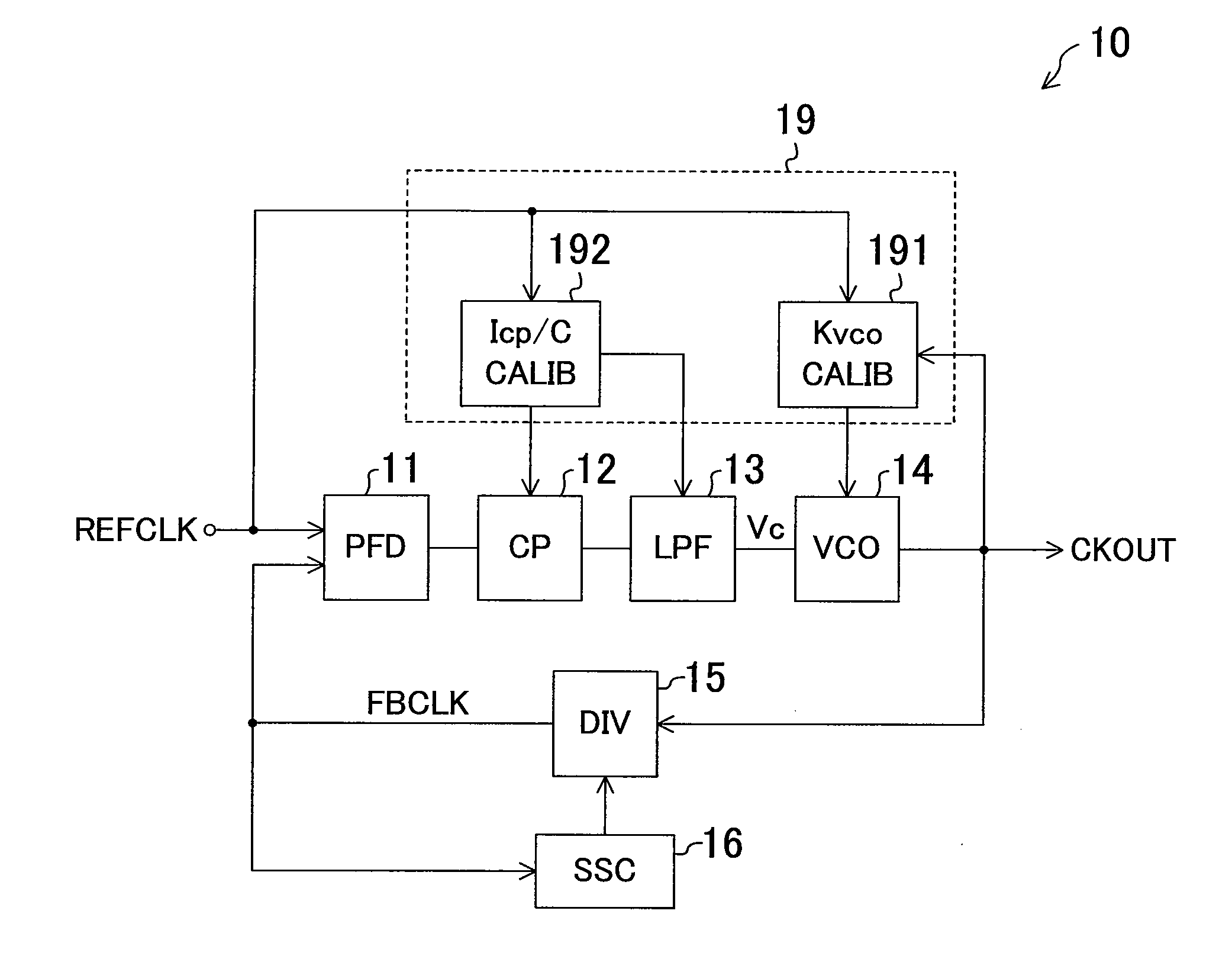
Spread spectrum control pll circuit and its start-up method
a technology of spread spectrum and control circuit, which is applied in the direction of automatic control, electrical equipment, etc., can solve the problems of increasing output distortion caused by spread spectrum modulation with a decrease in loop bandwidth, jitter or distortion is likely to increase, and the effect of simple configuration
- Summary
- Abstract
- Description
- Claims
- Application Information
AI Technical Summary
Benefits of technology
Problems solved by technology
Method used
Image

Examples
example configuration 1
of Calibration Circuit
[0063]FIG. 4 shows an example configuration of the circuit portion 191 of the calibration circuit 19. A timer circuit 1911 measures a period of time depending on the frequency of the reference clock signal REFCLK. Specifically, the timer circuit 1911 counts pulses of the reference clock signal REFCLK to a predetermined number N1. Thus, by setting the number of pulses to be counted to a fixed value, the timer circuit 1911 measures a short period of time when the input frequency is high, and a long period of time when the input frequency is low. In other words, the timer circuit 1911 measures a period of time which is proportional to the input frequency. A counter circuit 1912 counts pulses of the feedback clock signal FBCLK during a period of time when the timer circuit 1911 is operating. A memory circuit 1913 stores a count value of the counter circuit 1912 which is obtained when the H voltage is input as the control voltage of the VCO 14. The memory circuit 19...
example configuration 2
of Calibration Circuit
[0075]FIG. 8 shows an example configuration of the circuit portion 192 of the calibration circuit 19. An oscillator 1921 has a replica charge pump circuit (replica CP) 1922 which is a replica of the CP 12, and a filter capacitor 1923, and oscillates at a frequency (Icp / 2C) depending on a charging current Icp of the replica CP 1922 and a capacitance value C of and the filter capacitor 1923. A timer circuit 1924 measures a period of time depending on the frequency of the reference clock signal REFCLK. Specifically, the timer circuit 1924 counts pulses of the reference clock signal REFCLK to a predetermined number N3. A counter circuit 1925 counts pulses of an output clock signal CKOUT2 of the oscillator 1921 during a period of time when the timer circuit 1924 is operating. A comparator 1926 compares a count value of the counter circuit 1925 with a target value N4. A control circuit 1927 outputs the control signal REG2 based on an output of the comparator 1926 to ...
example configuration 3
of Calibration Circuit
[0087]FIG. 12 shows an example configuration of the circuit portion 192 of the calibration circuit 19. Only a difference between the circuit portion 192 of the calibration circuit 19 and the configuration 2 of the aforementioned calibration circuit, will be described. The oscillator 1921 has a charge pump circuit (CP) 1922′ and a replica filter capacitor (replica C) 1923′ which is a replica of the filter capacitor 131, and oscillates at a frequency (Icp / 2C) depending on a charging current Icp of the CP 1922′ and a capacitance value C of the replica C 1923′. The control circuit 1927 outputs the control signal REG2 to adjust the capacitance value of the replica C 1923′ based on the output of the comparator 1926. The control circuit 1927 also sets the capacitance values of the filter capacitor 131 and the replica C 1923′ in accordance with the common control signal REG2. In this case, it is not necessary to perform control to switch the charging current with respe...
PUM
 Abstract
Description
Claims
Application Information