Opto-electric hybrid board and manufacturing method thereof

a technology of opto-electric hybrid boards and manufacturing methods, which is applied in the direction of dielectric characteristics, inspection/indentification of circuits, instruments, etc., can solve the problems of difficult to obtain an image having a constant contrast, difficult to recognize, and long recognition time, so as to improve light propagation efficiency and easy to recognize. , the effect of high accuracy

Inactive Publication Date: 2010-05-27
NITTO DENKO CORP
View PDF7 Cites 16 Cited by
  • Summary
  • Abstract
  • Description
  • Claims
  • Application Information

AI Technical Summary

Benefits of technology

[0014]In the opto-electric hybrid board according to the present invention, the second alignment mark as a new alignment mark for the positioning of the optical element is formed on the surface of the electric circuit portion on which the optical element is mounted. The surface of the second alignment mark is covered with the resin layer, except for the uncovered portion serving as an identifying mark, by using the first alignment mark in the optical waveguide portion as a reference. Thus, the uncovered portion (the identifying mark) of the above-mentioned second alignment mark is also positioned relative to the end portion of the core, and may be used as a reference for the mounting position of the optical element. Additionally, covering the surface of the above-mentioned second alignment mark with the resin layer, except for the uncovered portion, allows the resin layer in the covered portion to be used to control luster and the like on the surface of the above-mentioned second alignment mark. For this reason, the above-mentioned uncovered portion exhibits a clear contrast to the portion covered with the resin layer, and it is easy to recognize the uncovered portion. As a result, the opto-electric hybrid board according to the present invention includes the optical element mounted with high accuracy to achieve improved light propagation efficiency.
[0015]In particular, when the above-mentioned second alignment mark is made of metal for an electric circuit, the luster on the surface of the above-mentioned second alignment mark is increased to provide a clearer contrast between the above-mentioned uncovered portion and the portion covered with the resin layer. This makes it easier to recognize the above-mentioned uncovered portion, thereby providing the optical element mounted with higher accuracy.
[0016]Also, in the method of manufacturing the opto-electric hybrid board according to the present invention, the second alignment mark as a new alignment mark for the positioning of the optical element is formed on the surface of the electric circuit portion on which the optical element is mounted, and the surface of the second alignment mark is covered with the resin layer, except for the uncovered portion serving as an identifying mark, by using as a reference the first alignment mark in the optical waveguide portion which is positioned relative to the end portion of the core. Thus, the uncovered portion (the identifying mark) of the above-mentioned second alignment mark is also positioned relative to the end portion of the core, and may be used as a reference for the mounting position of the optical element. Additionally, the uncovered portion of the above-mentioned second alignment mark exhibits a clear contrast to the portion covered with the resin layer as mentioned above, and it is easy to recognize the uncovered portion. As a result, false recognition is prevented, and the recognition is achieved in a short time, which results in improved productivity.
[0017]In particular, when the above-mentioned second alignment mark is formed using metal for the electric circuit, the second alignment mark is formed at the same time that the electric circuit is formed. This provides improved productivity. Additionally, the luster on the surface of the above-mentioned second alignment mark is increased to provide a clearer contrast between the above-mentioned uncovered portion and the portion covered with the resin layer. This makes it easier to recognize the above-mentioned uncovered portion, thereby further preventing the false recognition. Furthermore, the recognition is achieved in a shorter time.

Problems solved by technology

Light for illumination or the like is reflected diffusely because of the unevenness, and it tends to be difficult to obtain an image having a constant contrast.
For this reason, the recognition takes much time, and the mounting step requires a prolonged period of time.
Also, there is apprehension that false recognition results.

Method used


Image

  • Opto-electric hybrid board and manufacturing method thereof
  • Opto-electric hybrid board and manufacturing method thereof
  • Opto-electric hybrid board and manufacturing method thereof

Examples


example

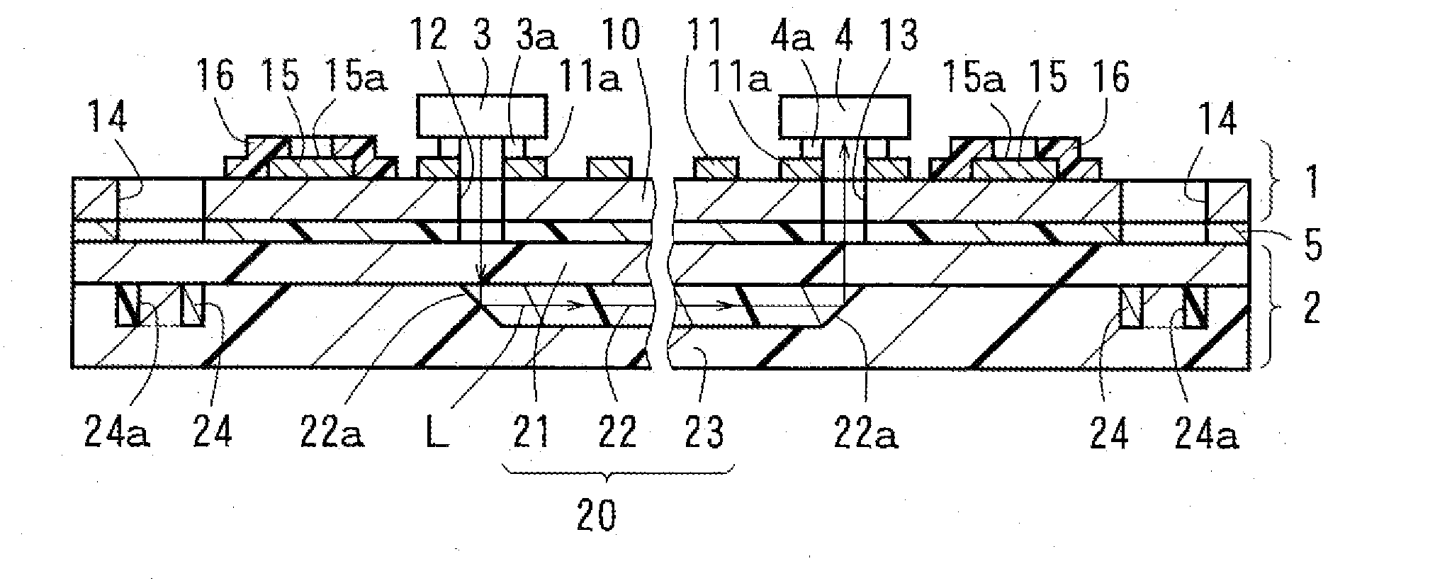
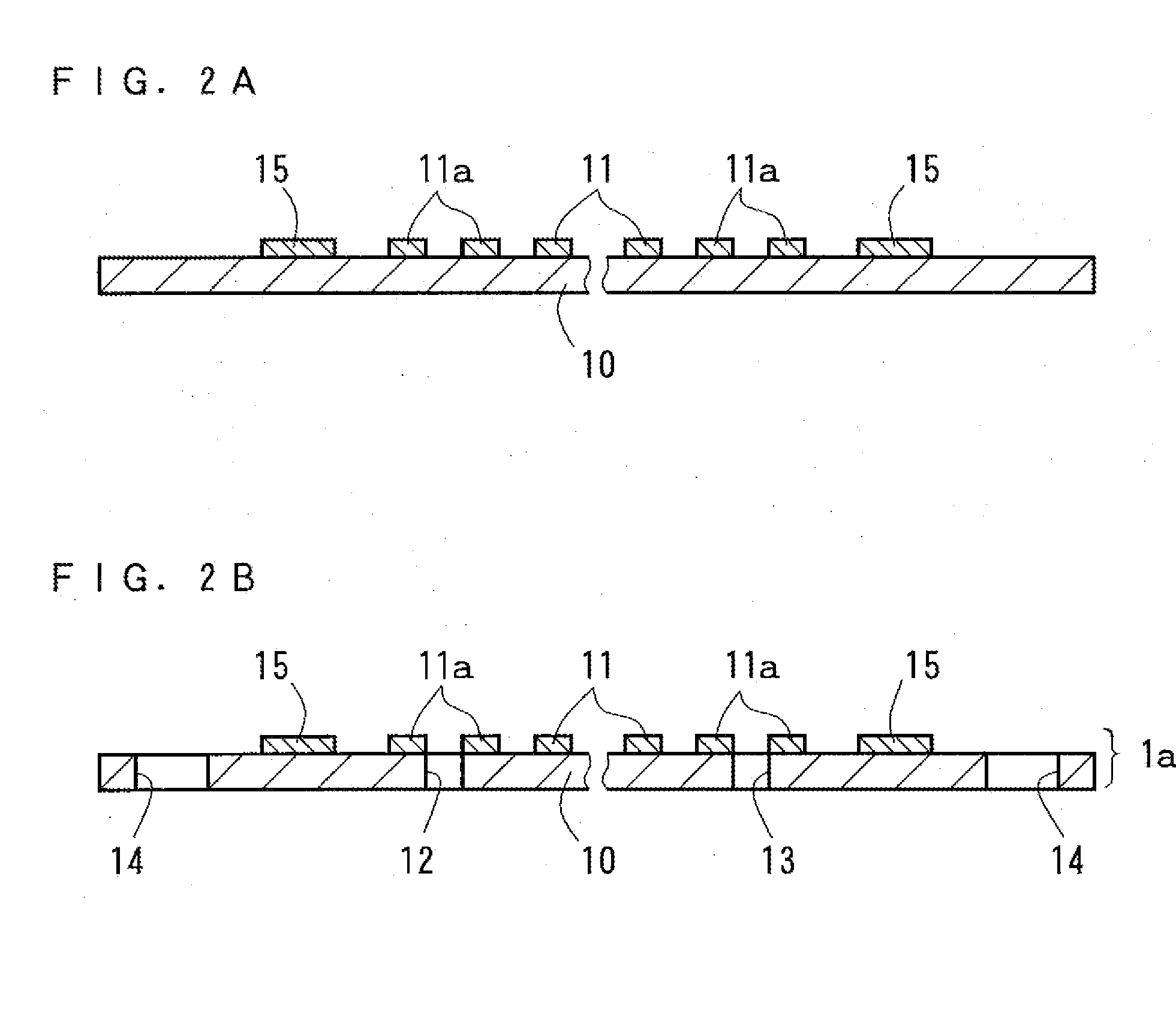
Electric Circuit Board

[0064]An electric circuit board was produced in which an insulation layer (having a thickness of 10 μm) made of a photosensitive polyimide resin was formed on one surface of a stainless steel plate material (SUS 304 foil having a thickness of 25 μm) and in which an electric circuit including mounting pads and second alignment marks were formed on a surface of the insulation layer, the electric circuit and the second alignment marks being formed by lamination of a seed layer made of an alloy of copper, nickel and chromium, and an electro copper plated layer. Through holes for light propagation and through holes for recognition of first alignment marks were formed in this electric circuit board.

Material for Formation of Under Cladding Layer and Over Cladding Layer

[0065]A material for formation of an under cladding layer and an over cladding layer was prepared by mixing 35 parts by weight of bisphenoxyethanol fluorene glycidyl ether (component A), 40 parts by weig...


PUM

PropertyMeasurementUnit
refractive indexaaaaaaaaaa

Abstract

An opto-electric hybrid board in which a new alignment mark having an identifying mark that is easy to recognize is formed in addition to a conventional alignment mark, and a method of manufacturing the opto-electric hybrid board. The opto-electric hybrid board includes an optical waveguide portion 2, an electric circuit board 1, and optical elements mounted on this electric circuit board 1. The optical waveguide portion 2 includes a translucent under cladding layer 21, a linear core 22 for an optical path, first alignment marks 24 positioned relative to end portions of this core 22, and an over cladding layer 23 for covering the above-mentioned core 22 and the first alignment marks 24. The electric circuit board 1 includes second alignment marks 15 for positioning of the optical elements and formed on a surface thereof on which the optical elements are mounted.

Description

RELATED APPLICATIONS[0001]This application claims the benefit of U.S. Provisional Application No. 61 / 120,635, filed Dec. 8, 2008, which is hereby incorporated by reference.BACKGROUND OF THE INVENTION[0002]1. Field of the Invention[0003]The present invention relates to an opto-electric hybrid board including an optical waveguide portion, an electric circuit portion, and an optical element mounted on this electric circuit portion, and to a manufacturing method thereof.[0004]2. Description of the Related Art[0005]An opto-electric hybrid board is constructed, for example, as shown in FIG. 7, by bonding an electric circuit portion 6 and an optical waveguide portion 7 to each other with an adhesive 5, and then mounting a light-emitting element 3 and a light-receiving element 4 on the above-mentioned electric circuit portion 6. The above-mentioned optical waveguide portion 7 includes an optical waveguide 70 in which an under cladding layer 71, a core 72, and an over cladding layer 73 are d...

Claims


Application Information

Patent Timeline
Patent Type & Authority Applications(United States)
IPC IPC(8): G02B6/12G02B6/13H05K3/00
CPCG02B6/42G02B6/4214G02B6/4224G02B6/43H05K1/0269Y10T29/49124H05K3/303H05K2201/0108H05K2201/09918H05K2203/063H05K2203/166H05K1/0274H05K2201/10121G02B6/12004G02B6/136G02B6/4201
Inventor HODONO, MASAYUKI
Owner NITTO DENKO CORP
Why Eureka
Try Eureka