Multilayer wiring substrate and method for manufacturing the same

a wiring substrate and multi-layer technology, applied in the direction of printed circuit aspects, conductive pattern formation, semiconductor/solid-state device details, etc., can solve the problems of difficulty in connecting solder bumps to surface connection terminals, difficulty in connecting ic chips directly onto motherboards, etc., to improve connection reliability, improve reliability, and improve the effect of reliability

Inactive Publication Date: 2010-06-03
NGK SPARK PLUG CO LTD
View PDF3 Cites 44 Cited by
  • Summary
  • Abstract
  • Description
  • Claims
  • Application Information

AI Technical Summary

Benefits of technology

[0008]The present invention has been accomplished in order to solve the above-described problem, and its object is to provide a method of manufacturing a multilayer wiring substrate which can improve reliability by improving the reliability of the connection between surface

Problems solved by technology

However, since the inter-terminal pitch differs greatly between the IC chip side terminal group and the motherboard side terminal group, difficulty is encountered in connecting the IC chip directly on

Method used


Image

  • Multilayer wiring substrate and method for manufacturing the same
  • Multilayer wiring substrate and method for manufacturing the same
  • Multilayer wiring substrate and method for manufacturing the same

Examples


Embodiment Construction

[0054]An exemplary embodiment of the present invention will now be described in detail with reference to the drawings.

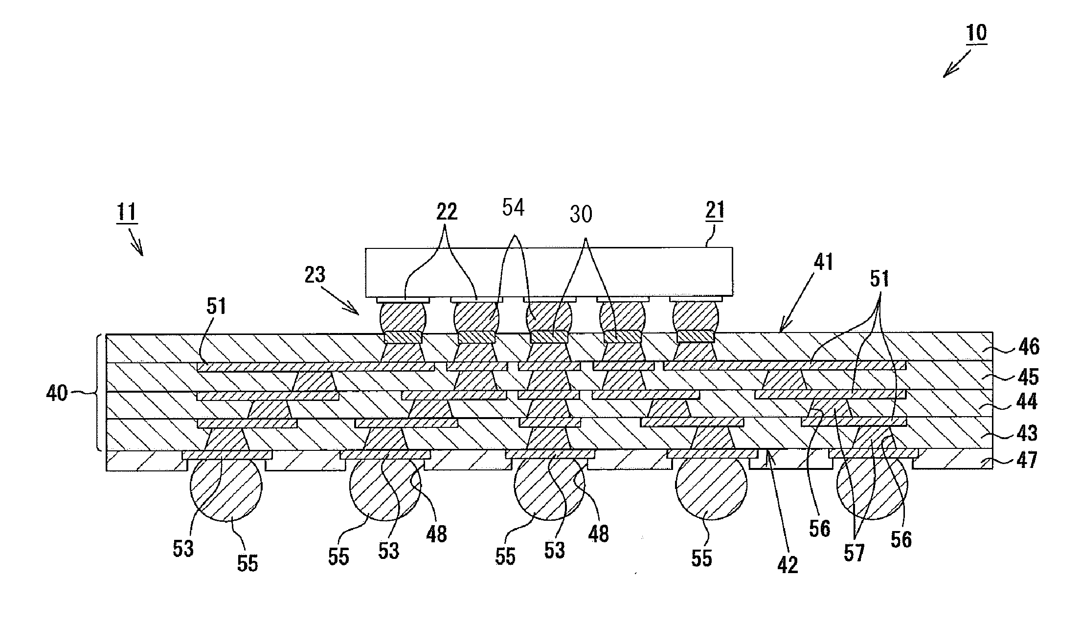
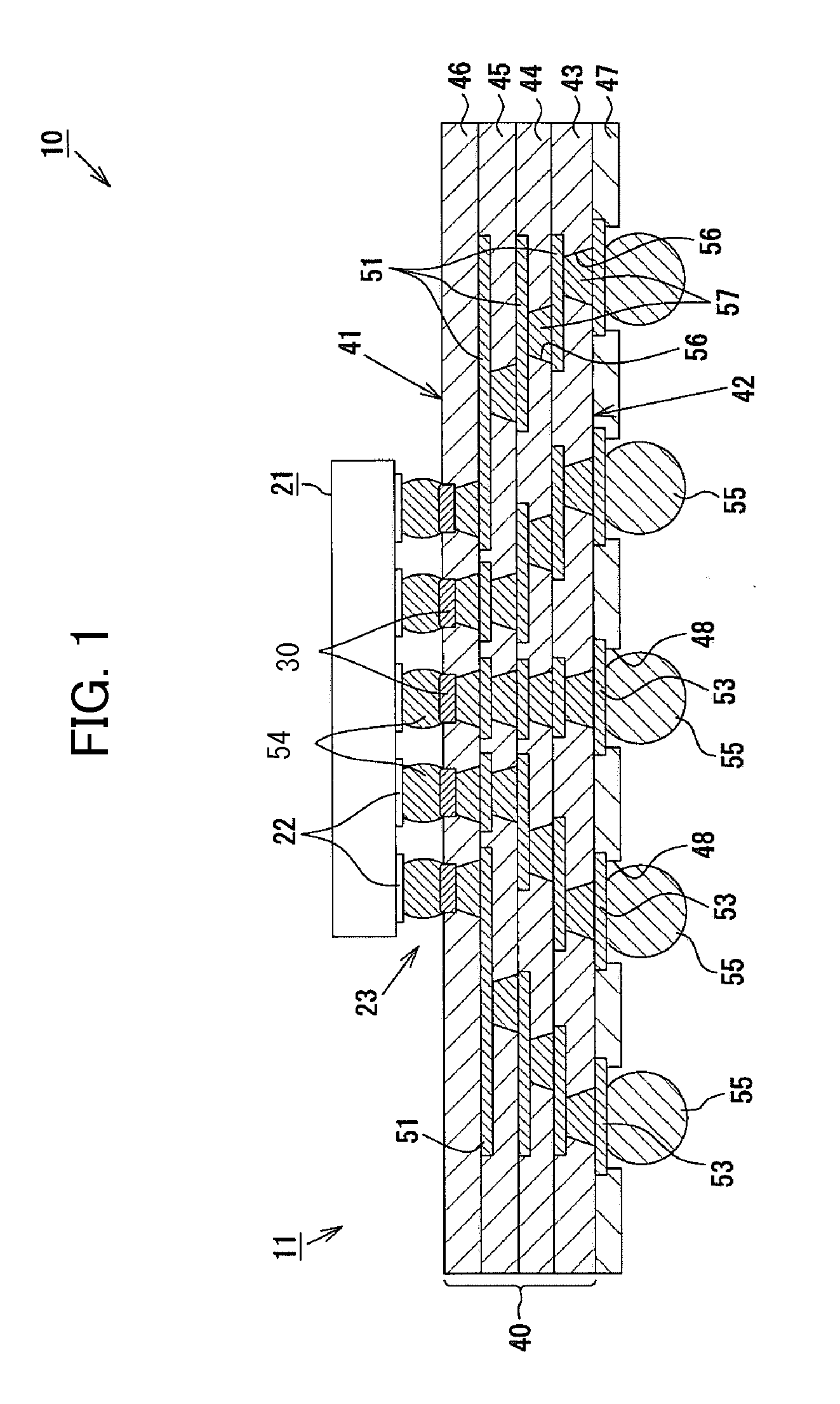
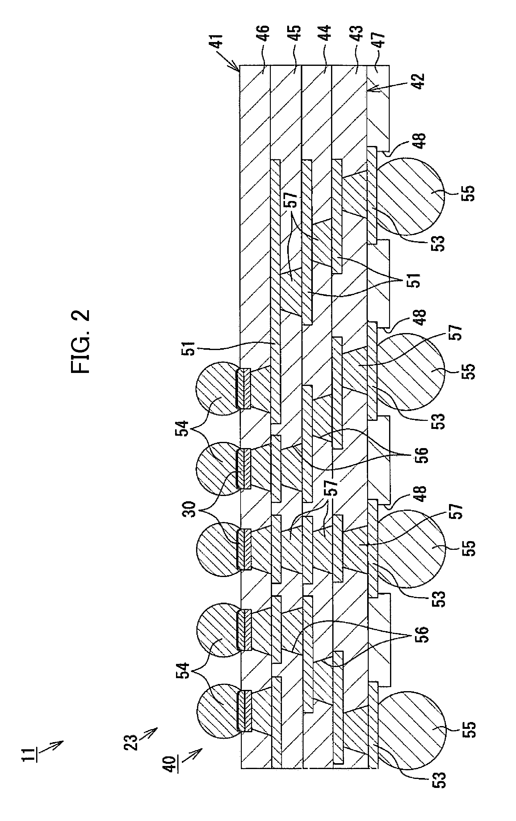
[0055]As shown in FIGS. 1 and 2, a semiconductor package 10 of the present embodiment is of a BGA (ball grid array) type, and is composed of a multilayer wiring substrate 11 and a IC chip 21 (chip component), which is a semiconductor integrated circuit element. Notably, the type of the semiconductor package 10 is not limited to BGA, and may be PGA (pin grid array), LGA (land grid array), or the like. The IC chip 21 is preferably formed of silicon whose coefficient of thermal expansion is 4.2 ppm / ° C. and assumes the form of a rectangular flat plate whose size is 15.0 mm (length)×15.0 mm (width)×0.8 mm (thickness).

[0056]Meanwhile, the exemplary multilayer wiring substrate 11 does not have a core substrate, and has a wiring stacked portion 40 (laminated structure) composed of conductor layers 51 formed of copper and four resin insulating layers 43, 44, 45, and 46, whic...


PUM

PropertyMeasurementUnit
Thicknessaaaaaaaaaa
Diameteraaaaaaaaaa

Abstract

A multilayer wiring substrate is manufactured through a recess forming step, a gold-diffusion-prevention-layer forming step, a terminal forming step, resin-insulating-layer forming step, a conductor forming step, and a metal-layer removing step. In the recess forming step, a copper foil layer is half-etched so as to form recesses. In the gold-diffusion-prevention-layer forming step, a gold diffusion prevention layer is formed in each recess. In the terminal forming step, a gold layer, a nickel layer, and a copper layer are stacked in sequence on the gold diffusion prevention layer to thereby form a surface connection terminal. In the resin-insulating-layer forming step, a resin insulating layer is formed, and, in the conductor forming step, via conductors and conductor layers are formed. In the metal-layer removing step, the copper foil layer and the gold diffusion prevention layer are removed so that the gold layer projects from the main face of the laminated structure.

Description

CROSS-REFERENCE TO RELATED APPLICATIONS[0001]This application is based on and claims priority to Japanese Patent Application No. JP2008-308445, filed Dec. 3, 2008, which is hereby incorporated by reference in its entirety.BACKGROUND OF THE INVENTION[0002]1. Field of the Invention[0003]The present invention relates to a multilayer wiring substrate having a laminated structure composed of conductor layers and resin insulating layers alternately stacked, and to a method for manufacturing the same.[0004]2. Description of Related Art[0005]In recent years, semiconductor integrated circuit elements (IC chips) used as microprocessors of computers or the like have been enhanced in speed and function more and more, and, thus, IC chips tend to have an increased number of terminals and a reduced inter-terminal pitch. In general, a large number of terminals are densely disposed in an array on the bottom surface of an IC chip. Such a group of terminals are flip-chip connected to a group of termin...

Claims


Application Information

Patent Timeline
IPC IPC(8): H01R12/00H05K3/10
CPCH01L23/49816Y10T29/49155H01L2221/68345H01L2224/16H01L2924/01046H01L2924/01078H01L2924/01079H01L2924/15174H01L2924/15311H05K3/0097H05K3/205H05K3/244H05K3/4007H05K3/4682H05K2201/0355H05K2201/0367H05K2203/0369H05K2203/1536H01L2924/1461H01L23/49822Y10T29/49162H01L2224/16235H01L2924/00H01L2224/0554H01L2224/05568H01L2224/05573H01L2924/00014H01L2224/05599H01L2224/0555H01L2224/0556
Inventor HANDO, TAKUYA
Owner NGK SPARK PLUG CO LTD
Why Eureka
Try Eureka