Thin film transistor, display unit, and method of manufacturing thin film transistor

a thin film transistor and display unit technology, applied in transistors, thermoelectric devices, solid-state devices, etc., can solve the problems of not being able to obtain favorable transistor characteristics, hardly providing oxygen to the oxide semiconductor thin film layer, etc., to achieve simple structure and manufacturing steps, reduce leakage current, and simplify manufacturing steps

Active Publication Date: 2010-06-03
JOLED INC
View PDF16 Cites 93 Cited by
  • Summary
  • Abstract
  • Description
  • Claims
  • Application Information

AI Technical Summary

Benefits of technology

[0010]However, in such a technique, since both protective films (the channel protective layer and the passivation film) are formed, two photolithography steps are necessitated. Further, before forming the passivation film, at least three high temperature heat steps (forming the channel protective layer, forming the source / drain electrode layer, and forming the passivation film) are performed. Thus, there has been the following disadvantage. That is, without whether or not oxygen detachment from the oxide semiconductor thin film layer is generated, after forming the passivation film, due to existence of the passivation film through which oxygen hardly passes, oxygen is hardly supplied to the oxide semiconductor thin film layer.
[0013]As described above, in the existing technologies, it has been difficult to decrease oxygen detachment in the oxide semiconductor thin film layer and to improve reliability with the use of a simple structure.
[0017]In the thin film transistor and the display unit of the embodiments of the invention, since the first channel protective layer is made of the oxide insulating material, and one or both of the first channel protective layer and the second channel protective layer is made of the low oxygen permeable material, oxygen detachment from the oxide semiconductor thin film layer is inhibited. Further, since the source / drain electrode is formed on the upper layer of the channel protective layer, oxygen detachment from the oxide semiconductor thin film layer is inhibited at the time of forming the source / drain electrode as well. Furthermore, since the channel protective layer has a function as the existing passivation film, the structure becomes simpler than the existing structure.
[0020]According to the thin film transistor, the display unit, and the method of manufacturing a thin film transistor of the embodiments of the invention, the channel protective layer that includes the first channel protective layer on the lower layer side and the second channel protective layer on the upper layer side is provided. Thus, at the time of forming the channel protective layer and the source / drain electrode, oxygen detachment from the oxide semiconductor thin film layer is able to be inhibited, and a leakage current is able to be decreased. Further, since the channel protective layer has a function as the existing passivation film, the structure and the manufacturing steps become simpler than the existing structure and the existing manufacturing steps. Thus, in the thin film transistor including the oxide semiconductor thin film layer, reliability is able to be improved with the use of a simple structure.

Problems solved by technology

That is, without whether or not oxygen detachment from the oxide semiconductor thin film layer is generated, after forming the passivation film, due to existence of the passivation film through which oxygen hardly passes, oxygen is hardly supplied to the oxide semiconductor thin film layer.
However, in such a technique, there is a disadvantage that oxygen detachment or the like is generated in a step of forming a source / drain electrode and thus favorable transistor characteristics are not able to be obtained.

Method used


Image

  • Thin film transistor, display unit, and method of manufacturing thin film transistor
  • Thin film transistor, display unit, and method of manufacturing thin film transistor
  • Thin film transistor, display unit, and method of manufacturing thin film transistor

Examples


first embodiment

1. First Embodiment

[0045](Structural Example of Display Unit)

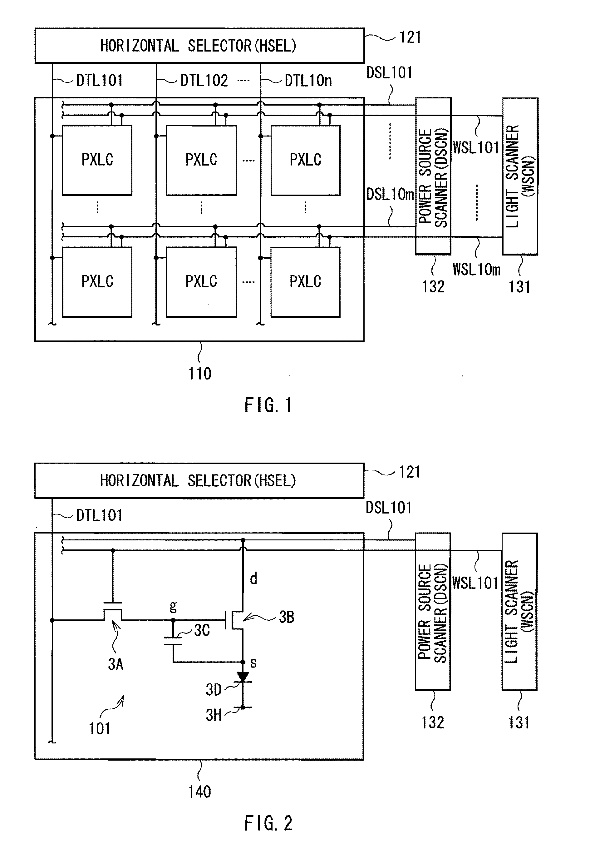
[0046]FIG. 1 illustrates a structure of a display unit according to a first embodiment of the invention. The display unit is used as an ultrathin organic light emitting color display unit or the like. In the display unit, for example, a display region 110 in which pixels PXLCs composed of a plurality of organic light emitting devices 10R, 10G, and 10B described later are arranged in a matrix state as a display device is formed in a TFT substrate 1. On the circumference of the display region 110, a horizontal selector (HSFL) 121 as a signal section, and a light scanner (WSCN) 131 and a power source scanner (DSCN) 132 as a scanner section are formed.

[0047]In the display region 110, signal lines DTL 101 to DTL 10n are arranged in the column direction, and scanning lines WSL 101 to WSL 10m and power source lines DSL 101 to DSL 10m are arranged in the row direction. A pixel circuit 140 including the organic light emitting devic...

second embodiment

2. Second Embodiment

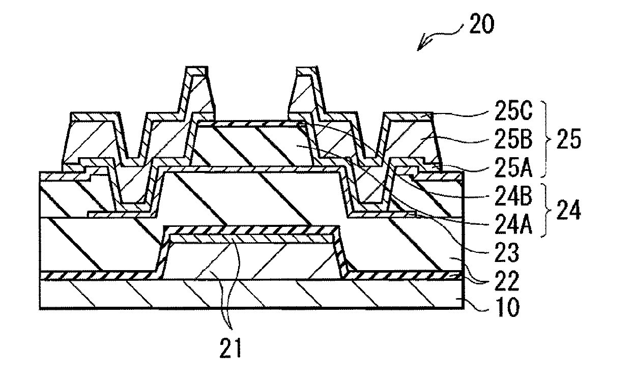
[0098](Structural Example of TFT)

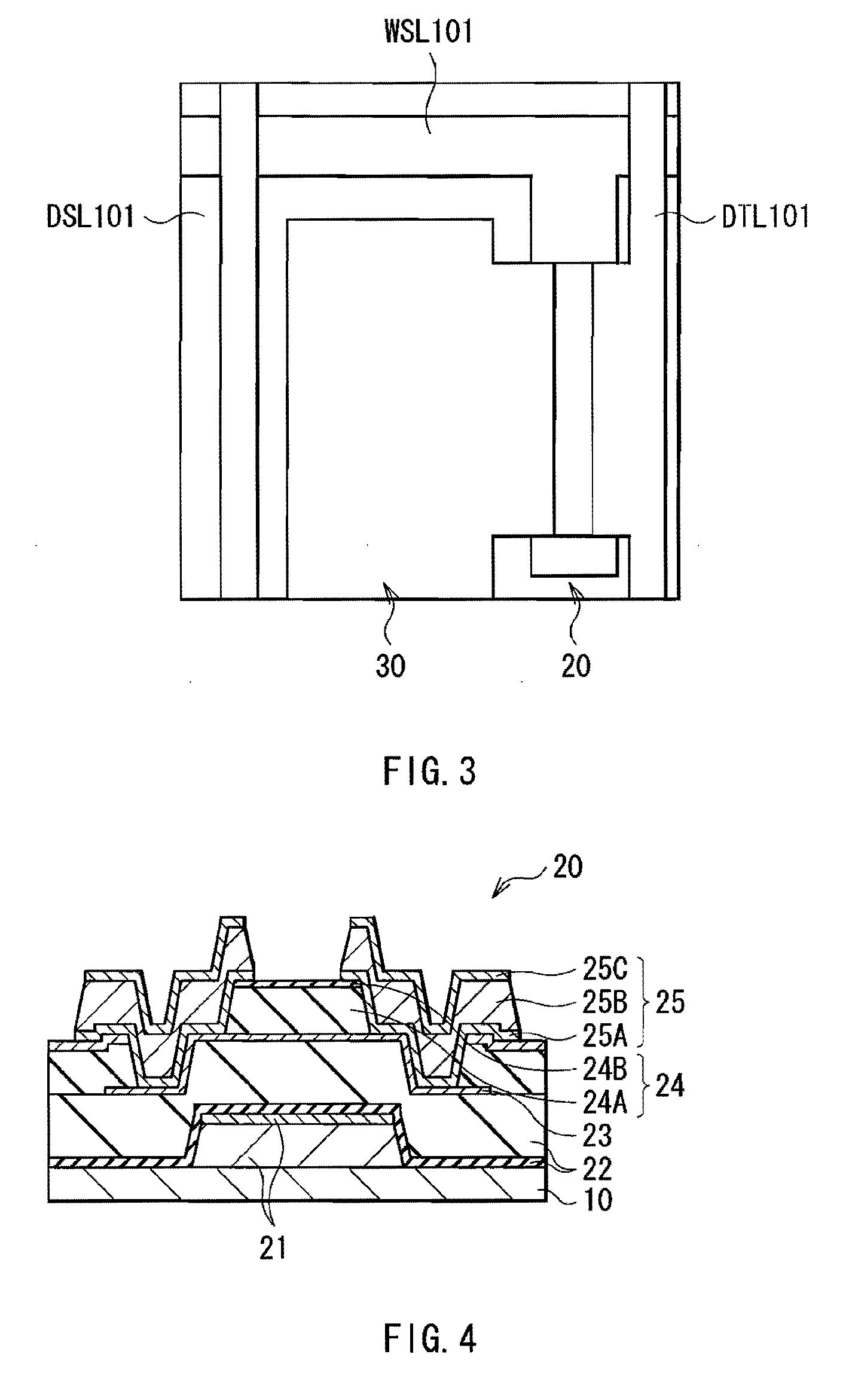
[0099]FIGS. 13A to 13C illustrate a planar structure of part of the pixel drive circuit 140 of the TFT substrate 1 according to a second embodiment of the invention (section corresponding to the sampling transistor 3A and the retentive capacity 3C of FIG. 2). This embodiment is totally the same as the foregoing first embodiment, except that a hole (aperture) described below is provided. Thus, a description will be given by affixing the same referential symbols to the corresponding elements.

[0100]First, in the foregoing first embodiment, in forming the TFT 20, at the time of forming the source / drain electrode 25, in some cases, there is a possibility that oxygen detachment from the oxide semiconductor thin film layer 23 is generated and the transistor characteristics are deteriorated.

[0101]Thus, in this embodiment, as in TFTs 20A to 20C illustrated in FIGS. 13A to 13C, at the time of pattering the channel protective layer 24 (at th...

application examples

3. Module and Application Examples

[0110]A description will be given of application examples of the display unit described in the foregoing embodiments. The display unit of the foregoing embodiments is able to be applied to electronic devices in any field such as a television device, a digital camera, a notebook personal computer, a portable terminal device such as a mobile phone, and a video camera. In other words, the display unit of the foregoing embodiments is able to be applied to a display unit of an electronic device in any field for displaying a video signal inputted from outside or a video signal generated inside as an image or a video.

Module

[0111]The display unit of the foregoing embodiments is incorporated in various electronic devices such as after-mentioned first to fifth application examples as a module as illustrated in FIG. 14, for example. In the module, for example, a region 210 exposed from the sealing substrate 71 and the adhesive layer 60 is provided in a side of...


PUM


Abstract

A thin film transistor includes: a gate electrode; a gate insulting film formed on the gate electrode; an oxide semiconductor thin film layer forming a channel region corresponding to the gate electrode on the gate insulating film; a channel protective layer that is formed at least in a region corresponding to the channel region on the gate insulating film and the oxide semiconductor thin film layer, and that includes a first channel protective layer on a lower layer side and a second channel protective layer on an upper layer side; and a source / drain electrode that is formed on the channel protective layer and is electrically connected to the oxide semiconductor thin film layer. The first channel protective layer is made of an oxide insulating material, and one or both of the first channel protective layer and the second channel protective layer is made of a low oxygen permeable material.

Description

BACKGROUND OF THE INVENTION[0001]1. Field of the Invention[0002]The present invention relates to a thin film transistor (TFT) including an oxide semiconductor thin film layer, a method of manufacturing the same, and a display unit including such a thin film transistor.[0003]2. Description of the Related Art[0004]It has been known that an oxide (oxide semiconductor) composed of zinc, indium, gallium, tin, or a mixture thereof shows superior semiconductor characteristics. Thus, in recent years, applying the oxide semiconductor to a TFT as a drive element of an active matrix display has been actively studied.[0005]In the TFT including the oxide semiconductor, electron mobility ten times or more of that of the existing TFT including amorphous silicon is shown and favorable off-characteristics are shown. Thus, the TFT including the oxide semiconductor is largely expected to be applied to a large-screen, high-definition, and high-frame-rate liquid crystal display and an organic EL display...

Claims


Application Information

Patent Timeline
Patent Type & Authority Applications(United States)
IPC IPC(8): H01L29/786H01L51/52H01L21/34
CPCH01L27/1225H01L29/7869H01L27/3262H10K59/1213
Inventor ARAI, TOSHIAKIMOROSAWA, NARIHIROTOKUNAGA, KAZUHIKO
Owner JOLED INC
Why Eureka
Try Eureka