Semiconductor Package Leads Having Grooved Contact Areas

a technology of contact area and semiconductor, which is applied in the direction of printed circuit aspects, sustainable manufacturing/processing, final product manufacturing, etc., can solve the problems of erratic oxidation of the base metal at the cut line, inconsistent and unreliability of the solder wet solder, and erratic wettability of the solder. , to achieve the effect of significant yield saving and reliability of the assembled devi

Inactive Publication Date: 2010-06-03
TEXAS INSTR INC
View PDF0 Cites 43 Cited by
  • Summary
  • Abstract
  • Description
  • Claims
  • Application Information

AI Technical Summary

Benefits of technology

[0007]It is a technical advantage of the invention that no process or material change of the device is required, only the tool for stamping or etching the leadframe has to be modified. On the other hand, the impact of the invention on yield saving and reliability of the assembled device is significant.
that no process or material change of the device is required, only the tool for stamping or etching the leadframe has to be modified. On the other hand, the impact of the invention on yield saving and reliability of the assembled device is significant.

Problems solved by technology

Applicant found in the assembly step of the devices that solder is wetting the saw-exposed base metal at the cut line only inconsistently and unreliably.
Applicant's analysis of the exposed metal surface revealed erratic oxidation of the base metal and consequently erratic wettability by solder.
Thus, the inspection has to declare a yield loss even if the device is actually an electrically good device.

Method used


Image

  • Semiconductor Package Leads Having Grooved Contact Areas
  • Semiconductor Package Leads Having Grooved Contact Areas
  • Semiconductor Package Leads Having Grooved Contact Areas

Examples


Embodiment Construction

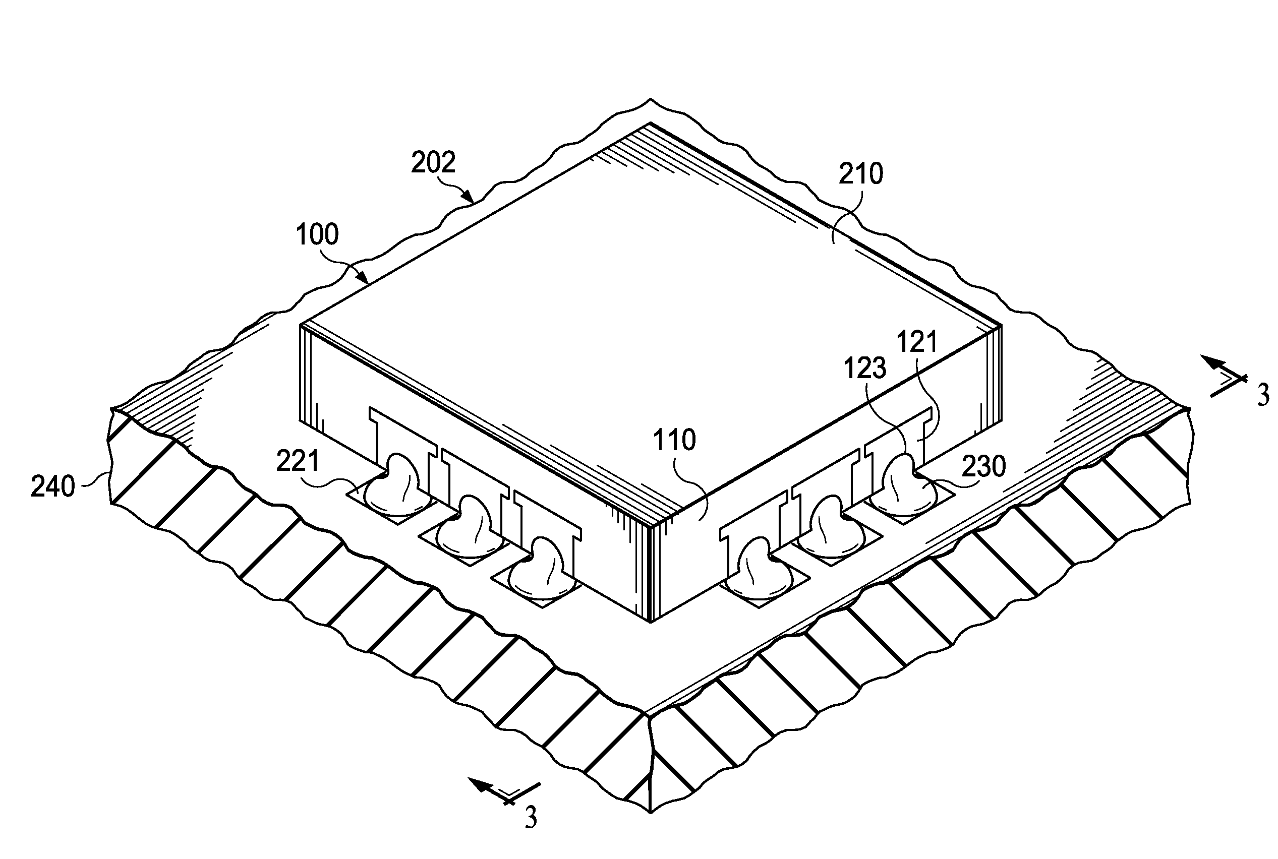
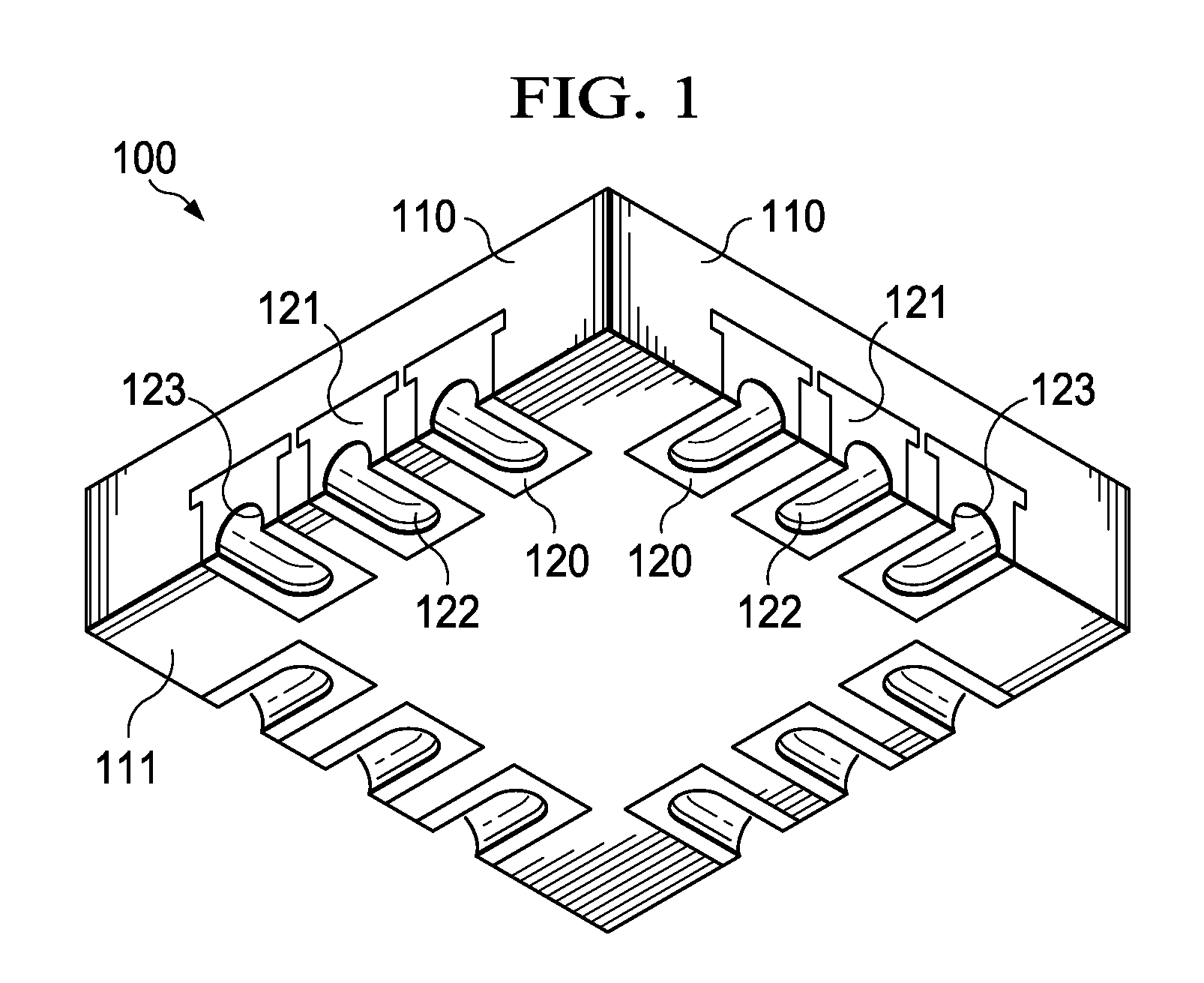
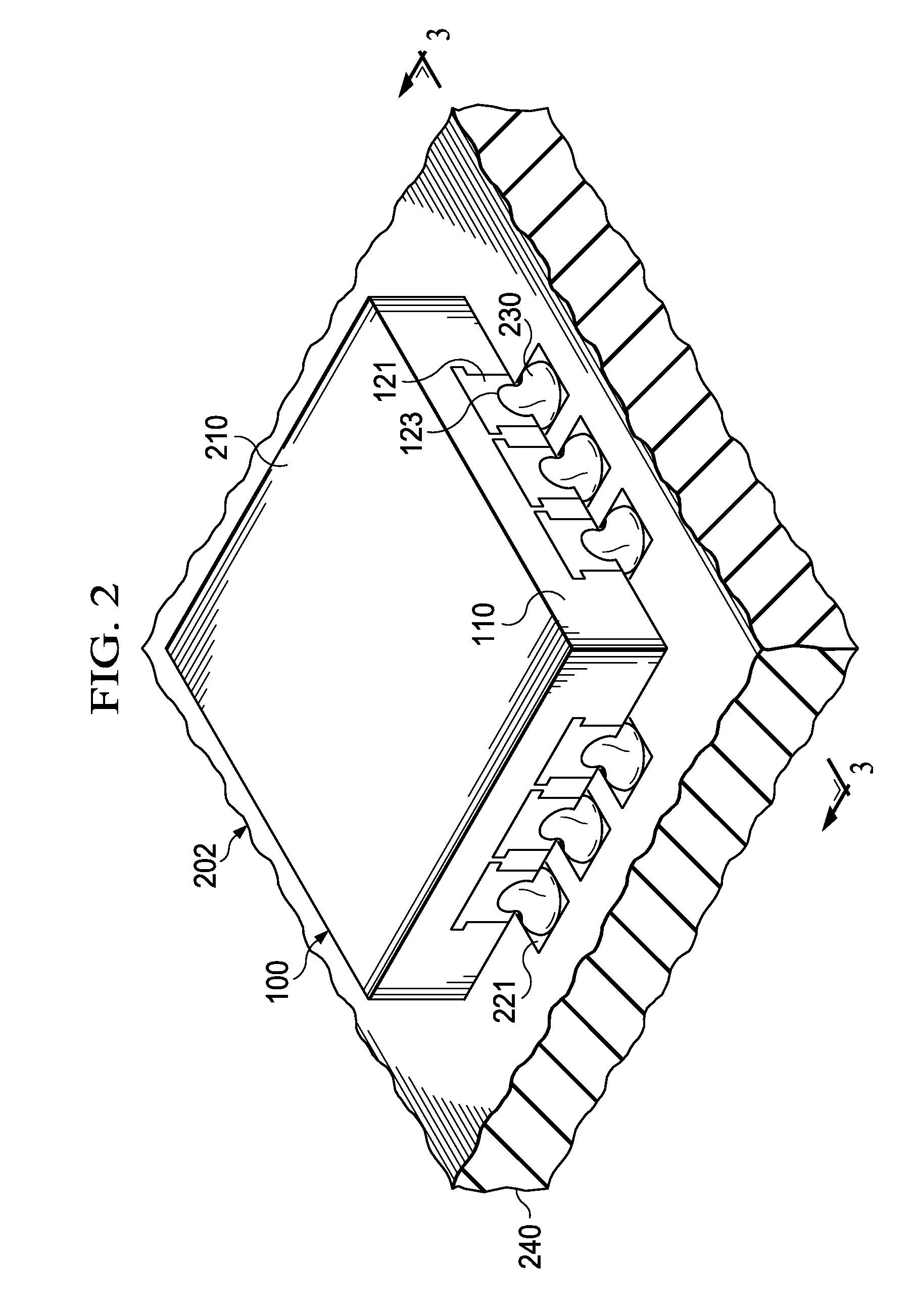
[0017]FIG. 1 is a schematic perspective view of the bottom surface of an exemplary semiconductor device, generally designated 100, of the Small Outline No-Lead (SON) or Quad Flat No-Lead (QFN) family. The device is packaged in an insulating encapsulation material, preferably a molding compound, and has metal terminals 120, preferably made of copper or a copper alloy as the base metal. The SON / QFN device family covers a wide spectrum of device shapes (usually hexahedron, square or rectangular cross section), sizes (length less than 1 mm to more than 10 mm), and numbers and distributions of terminals. To mention only a few examples of the terminal numbers, SON / QFN devices sized 4 mm×4 mm may have 16 or 24 terminals; devices sized 5 mm×5 mm may have 16, 20, or 32 terminals; devices sized 6 mm×6 mm may have 20 or 28 terminals; devices sized 7 mm×7 mm may have 32 or 44 terminals; and a device sized 8 mm×8 mm may have 56 terminals. In the latter example, the pitch center-to-center of the ...


PUM


Abstract

A packaged semiconductor device (100) has a first (110) and a second (111) side, the second side including a plurality of metal terminals (120) extending to the first side. Each terminal includes an oblong groove (122) extending to the first side and ending in an orifice (123) at the first side. The terminals are made of a base metal and may have a solder-wettable surface except for the terminal surface (121) exposed at the first device side.

Description

FIELD OF THE INVENTION[0001]The present invention is related in general to the field of semiconductor devices and processes, and more specifically to the structure and fabrication method of Small Outline No-Lead (SON) and Quad Flat No-Lead (QFN) devices having solder contact areas enlarged by grooves.DESCRIPTION OF RELATED ART[0002]Semiconductor Small Outline No-Lead (SON) and Quad Flat No-Lead (QFN) devices are typically fabricated by assembling a plurality of chips on a strip of metallic leadframe. The leadframe is laid out to include for each device the needed chip pads and coordinated lead segments. In order to miniaturize the devices and conserve area in the layout of the leadframe strip, the layout is commonly designed so that the segments of one device are connected directly to the respective segments of the adjacent devices.[0003]The majority of leadframes is made of a base metal such as copper or an alloy including copper, and plated with layers of solderable metal, such as...

Claims


Application Information

Patent Timeline
Patent Type & Authority Applications(United States)
IPC IPC(8): H01L23/488H01L21/50
CPCH01L21/561H01L24/48H01L23/49503H01L23/49548H01L23/49582H01L2224/32245H01L2224/48091H01L2224/48247H01L2224/48465H01L2224/73265H01L2924/01029H01L2924/01046H01L2924/01078H01L2924/01079H05K3/3426H05K3/3442H05K2201/10727H05K2201/1084H01L2224/97H01L24/97H01L2924/01087H01L23/3107H01L2924/00014H01L2924/00H01L2924/181H01L2924/14Y02P70/50H01L2924/18301H01L2924/00012H01L2224/45099H01L2224/45015H01L2924/207
Inventor ARSHAD, MOHAMAD ASHRAF MOHD
Owner TEXAS INSTR INC
Why Eureka
Try Eureka