Low resistance through-wafer via

Active Publication Date: 2010-06-03
SILEX MICROSYST
View PDF5 Cites 45 Cited by
  • Summary
  • Abstract
  • Description
  • Claims
  • Application Information

AI Technical Summary

Benefits of technology

[0019]It is a further advantage of the invention to provide a plated through-wafer via which can be selected to be open or closed, i.e. a hermetically sealed through-wafer via is possible.
[0020]It is a yet further advantage that the constriction of the through-wafer via provides an improved adhesion of the conductive material and gives a mechanical support to the conductive material, improving the robustness and the reliability

Problems solved by technology

The prior art has drawbacks with regards to being able to provide reliable, low resistance through-wafe

Method used


Image

  • Low resistance through-wafer via
  • Low resistance through-wafer via
  • Low resistance through-wafer via

Examples


Embodiment Construction

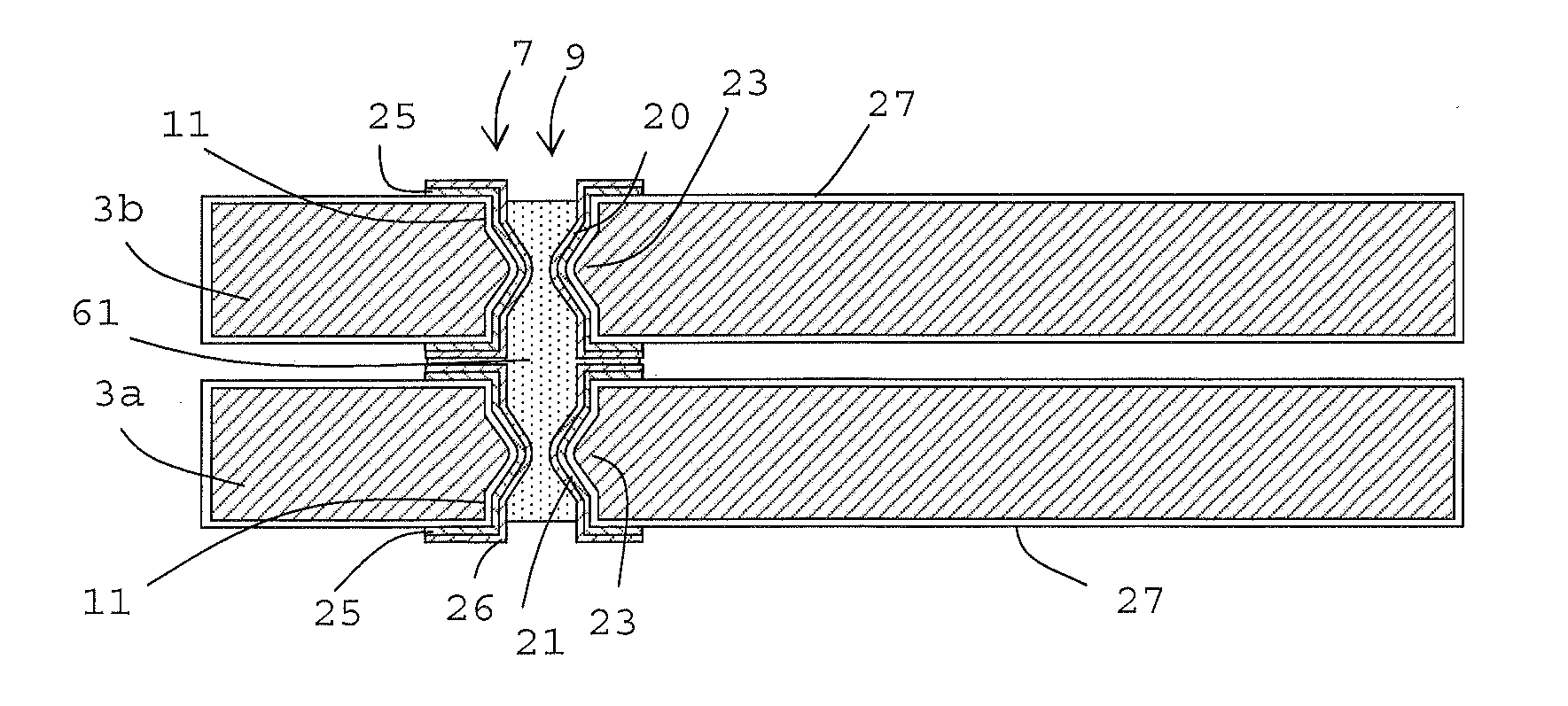
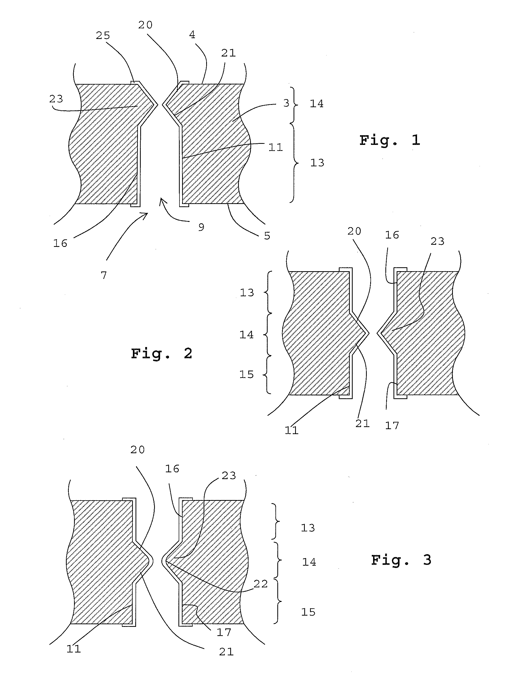
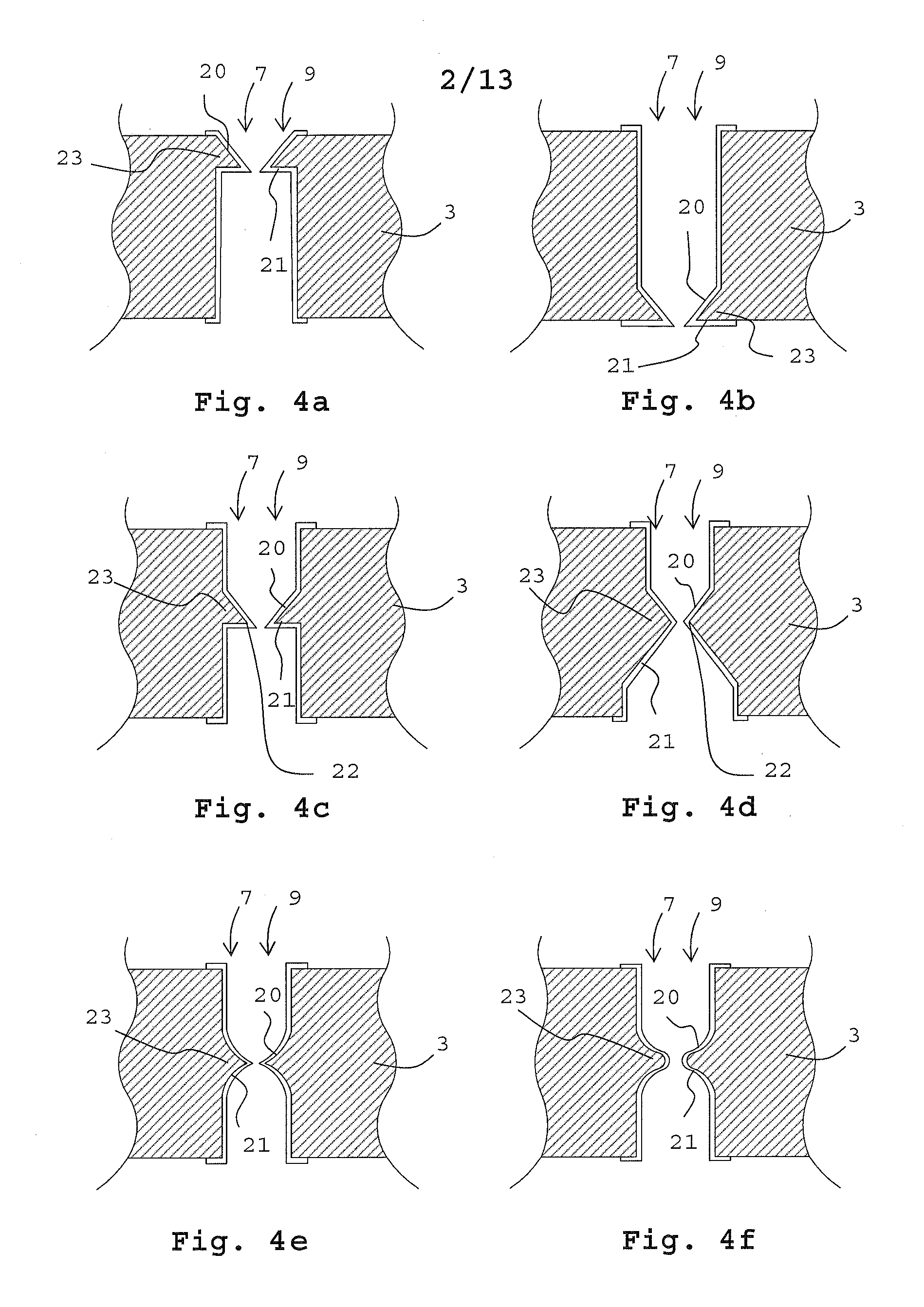
[0046]For the purpose of this application the term “electronic device” refers to microelectronic devices, electronic MEMS devices, electronic nanotechnology devices, as well as simpler electronic devices. A microelectronic device may comprise microelectronic components such as integrated circuits integrated in the wafer surface or arranged on the surface of the wafer. A MEMS device may be formed by micromachining of e.g. a semiconductor wafer or surface micromachining on a wafer. The simpler electronic device may be a substrate used as a carrier for electronic components or an intermediate layer between other electronic devices. The term “wafer” originates from the fact the electronic devices such as integrated circuits and mostly also MEMS structures are made from silicon wafers. However the term wafer is not limited to silicon wafers or circular substrates, which is the typical shape of silicon wafers, but refers to all substrates suitable for use in electronic devices.

[0047]The d...


PUM


Abstract

The present invention provides a wafer (3) comprising a through-wafer via (7) through the wafer (3) formed by a through-wafer via hole (9) and at least a first conductive coating (25). A substantially vertical sidewall (11) of the through-wafer via hole (9) except for a constriction (23) provides a reliable through-wafer via (7) occupying a small area on the wafer. The wafer (3) is preferably made of a semiconductor material, such as silicon, or a glass ceramic. A method for manufacturing such a wafer (3) is described.

Description

TECHNICAL FIELD OF THE INVENTION[0001]The present invention relates to electrically conductive connections through a wafer used for electronic devices, such as a silicon wafer or a glass wafer.BACKGROUND OF THE INVENTION[0002]In microelectronics integrated circuit device density is increasing at a high rate. In 1965 Moore's law predicted that the number of transistors per chip would double every 2 years, and the development of microelectronics has indeed roughly matched this prediction. However the implementation of further miniaturization of integrated circuits is costly and the ever more complex circuits require an increasing number of I / O leads, which complicates the contacting and packaging of the devices. Hence other means for getting higher device density are needed. An emerging alternative is to increase the device density per unit area by stacking devices on top of each other. Currently, stacked devices are mostly interconnected by wire bonding, which is a complex process th...

Claims


Application Information

Patent Timeline
IPC IPC(8): H01L23/538H01L21/768
CPCB81B2207/07B81C1/00095H01L2924/0002H01L21/76898H01L23/481H01L23/49827H01L25/0657H01L25/50H01L2225/06513H01L2225/06541H01L2924/09701H01L2924/12044H05K1/0306H05K3/002H05K3/0041H05K3/4076H05K3/42H05K2201/09827H05K2201/09854H01L2924/00
Inventor NILSSON, PETER
Owner SILEX MICROSYST
Why Eureka
Try Eureka