Plasma etching apparatus and method

a technology of etching apparatus and plasma, which is applied in the direction of electrical equipment, basic electric elements, semiconductor/solid-state device manufacturing, etc., can solve the problems of difficult control of etching profile, difficult to obtain uniform etching rate, etc., and achieve high integration of semiconductor devices and effective use

Inactive Publication Date: 2010-06-10
TOKYO ELECTRON LTD
View PDF6 Cites 2 Cited by
  • Summary
  • Abstract
  • Description
  • Claims
  • Application Information

AI Technical Summary

Benefits of technology

[0011]In accordance with the plasma etching apparatus of the first aspect of the present invention, the ring-shaped protrusion is provided on the bottom surface of the shower head and, also, the gas introducing openings are inclusively arranged in the inner central portion of the ring-shaped protrusion. With the presence of the ring-shaped protrusion, the uniform pressure is obtained in the plasma generation space. Accordingly, it is possible to control the plasma density and the amount of deposits especially in the vicinity of the ring-shaped protrusion. Further, the exclusive arrangement of the gas introducing openings in the central portion increases the gas velocity in the space above the central portion of the target object, which leads to a suppression of the generation of etchants in the central portion. As a result, it is possible to obtain the intra-surface uniformity of the etching rate and control the etching profile.
[0012]In accordance with the first aspect of the present invention, it is preferable to form a pair of facing electrodes by using the mounting table as a lower electrode and the shower head as an upper electrode. Preferably, an outer diameter of the ring-shaped protrusion is about 1.1 to about 1.5 times a diameter L of the target object. Further, preferably, an inner diameter of the ring-shaped protrusion is greater than the diameter L of the target object. Accordingly, a plasma generation space is formed in a space above the target object, so that the intra-surface etching uniformity can be ensured.
[0013]Preferably, a height of the ring-shaped protrusion is equal to or greater than about 0.4 times a distance from the mounting table to the shower head. Accordingly, the conductance of the gas flow is reduced, so that the uniform pressure is obtained in the space surrounded by the ring-shaped protrusion. Further, preferably, the gas introducing openings are inclusively formed in an area of about 0.3 L×0.3 L to about 0.7 L×0.7 L, L being a diameter of the target object. Therefore, the gas velocity can be sufficiently increased in the space above the central portion of the target substrate.
[0018]The plasma etching apparatus of the present invention has on the bottom surface of the shower head the ring-shaped protrusion protruded toward the mounting table and the multiple gas introducing openings inclusively distributed in an area smaller than the target object. By using such a plasma etching apparatus, it is possible to obtain the uniform etching depth in the surface of the target object and control the etching to be carried out in a tapered shape. Since the plasma etching apparatus can be effectively used for manufacturing high-reliability semiconductor devices, it is possible to cope with a miniaturization and a high integration of the semiconductor devices.

Problems solved by technology

However, in case silicon is etched when a resist is used as a mask, it is difficult to obtain a uniform etching rate (i.e., a depth of a hole) in a surface of a semiconductor wafer serving as a target substrate and an etching profile is difficult to control.

Method used


Image

  • Plasma etching apparatus and method
  • Plasma etching apparatus and method
  • Plasma etching apparatus and method

Examples


experimental example 1

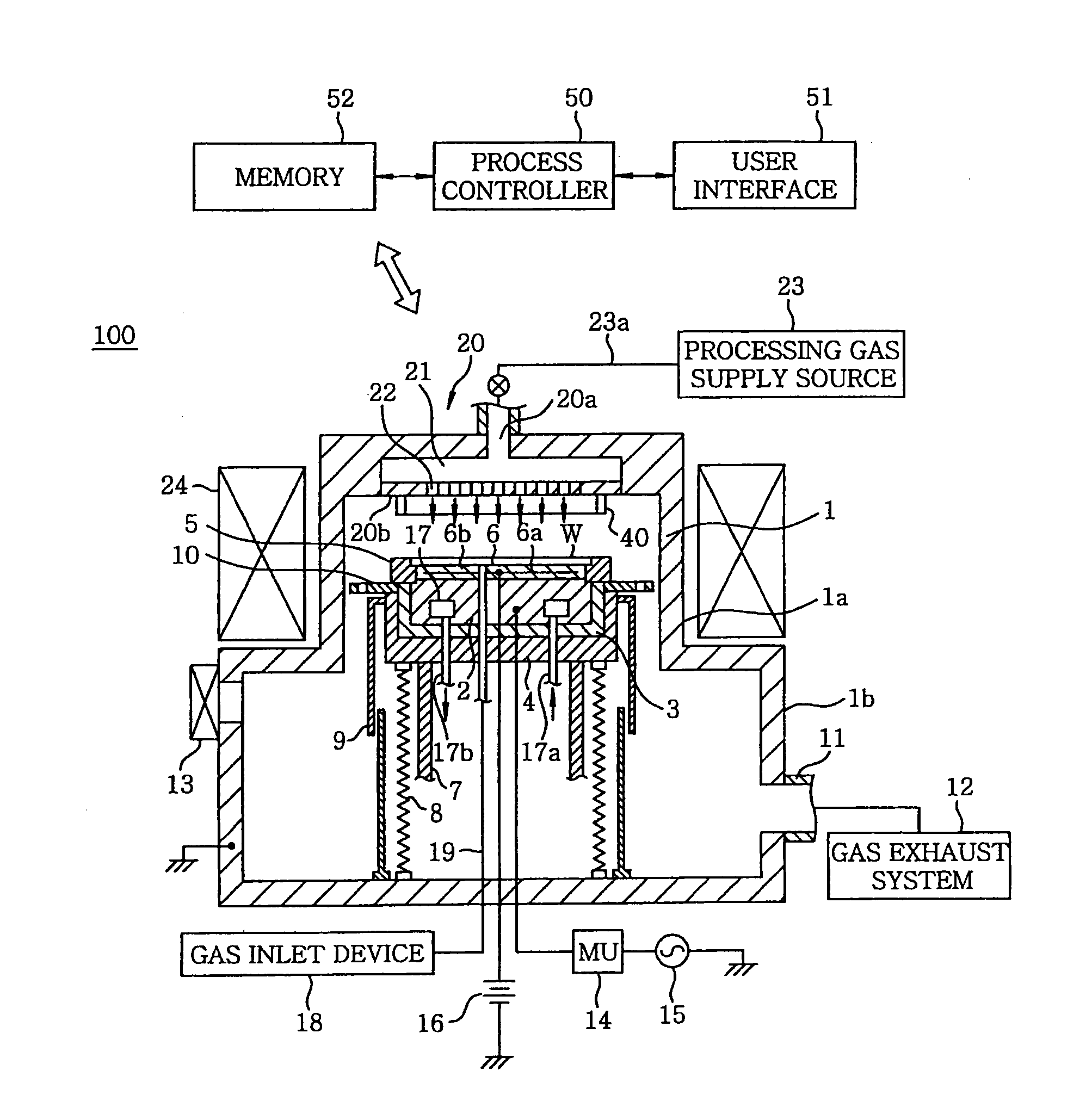
[0064]A plasma etching process was performed on the target object 110 having the structure of FIG. 6 by using the shower head 20 having the ring-shaped protrusion 40 of two sizes, A and B to be described below, thereby forming the hole 121 on the silicon substrate 101. A distance G (gap) between the upper and the lower electrode was set to be 22 mm, 27 mm and 32 mm. As for the shower head 20, one having an alumite treated surface was used.

[0065]Ring-shaped protrusion A:

[0066]Protruding amount H=15 mm

[0067]Outer diameter L1=260 mm

[0068]Inner diameter L2=240 mm

[0069]Width [(L1−L2)×½]=10 mm

[0070]Ring-shaped protrusion B:

[0071]Protruding amount H=21 mm

[0072]Outer diameter L1=270 mm

[0073]Inner diameter L2=240 mm

[0074]Width [(L1−L2)×½]=15 mm

[0075]The etching was performed under following conditions:

[0076]Resist: film thickness=7 μm

[0077]Processing gas: SF6 / O2=170 / 50 mL / min (sccm)

[0078]Pressure=37.3 Pa (280 mTorr)

[0079]RF frequency (high frequency power supply 15)=40 MHz

[0080]RF power=840 ...

experimental example 2

[0087]Under the same conditions as those of the experimental example 1, a plasma etching process was performed on the target object 110 having the structure of FIG. 6 by using the shower head 20 having 49 gas inlet openings 22 inclusively in an area S of about 108.7 mm2 in the central portion of the bottom surface 20b thereof while setting a distance (gap) G between the upper and the lower electrode at about 22 mm, 27 mm, 32 mm or 33 mm, thereby forming the hole 121 on the silicon substrate 101. Further, the etching depth of the hole 121 was evaluated in terms of the intra-wafer uniformity. A result thereof will be shown in Table 2. The good intra-surface uniformity of the etching depth is indicated as “o”, whereas the poor intra-surface uniformity thereof is indicated as “x”.

TABLE 2Ring-shapedGap (mm)Protrusions222732A◯——B◯——B—◯—B——X

[0088]As described in Table 2, in case of the shower head 20 having 49 gas inlet openings 22 inclusively in the area S of about 108.7 mm2, the good int...

experimental example 3

[0089]Under the same conditions as those of the experimental example 1, a plasma etching process was performed on the target object 110 having the structure of FIG. 6 by using the shower head 20 having a Y2O3 thermally sprayed coating surface, thereby forming the hole 121 on the silicon substrate 101. At this time, a size of the area S containing all of the gas introducing openings inclusively in the central portion of the bottom surface 20b and the number of the gas introducing openings 22 disposed therein were varied, as illustrated in Table 3. In this experiment, the distance (gap) G between the upper and the lower electrode was set to be 37 mm, and the ring-shaped protrusion 40 was not provided. Further, the etching depth of the hole 121 was evaluated in terms of the intra-wafer uniformity. A result thereof will be shown in Table 3. The good intra-wafer uniformity of the etching depth is indicated as “o”, whereas the poor intra-wafer uniformity thereof is indicated as “x”.

TABLE ...


PUM


Abstract

A plasma etching apparatus includes an evacuable processing chamber for performing a plasma etching process on a target object; a mounting table for mounting thereon the target object in the processing chamber; and a shower head facing the mounting table, for introducing a processing gas for generating a plasma to the processing chamber. Further, the apparatus includes a ring-shaped protrusion protruded from a bottom surface of the shower head toward the mounting table; and a plurality of gas introducing openings inclusively arranged in an area smaller than the target object in an inner central portion of the ring-shaped protrusion on the bottom surface of the shower head.

Description

CROSS-REFERENCE TO RELATED APPLICATIONS[0001]This application is a divisional of U.S. Application Ser. No. 11 / 678,833, filed on Feb. 26, 2007, the entire content of which is incorporated herein by reference, and claims priority under 35 U.S.C. 119 to Japanese Patent Application No. 2006-049639, filed on Feb. 27, 2006, and U.S. Provisional Application No. 60 / 779,969 filed on Mar. 8, 2006.FIELD OF THE INVENTION[0002]The present invention relates to a plasma etching apparatus and method; and, more particularly, to a plasma etching apparatus and method for use in etching a target object by using a plasma.BACKGROUND OF THE INVENTION[0003]A manufacturing process of a semiconductor device such as a three-dimensional stack package device or the like includes a silicon etching for forming wiring through holes, mechanical structure grooves or the like.[0004]As for the above silicon etching, there has been generally employed a silicon etching method including the steps of: etching an oxide fil...

Claims


Application Information

Patent Timeline
Patent Type & Authority Applications(United States)
IPC IPC(8): H01L21/3065
CPCH01L21/32137H01L21/3065
Inventor NAKAYA, MICHIKOMARUYAMA, KOJI
Owner TOKYO ELECTRON LTD
Why Eureka
Try Eureka