High temperature and high voltage electrode assembly design

a high-temperature and high-voltage technology, applied in the field of electrodes, can solve the problems of electrodes having a ripple effect on the cost of operation, easy damage, increased risk of failure, etc., and achieve the effects of reducing the time required to heat up the reaction chamber, improving throughput, and increasing electrical voltag

Inactive Publication Date: 2010-06-17
GTSP GLOBAL
View PDF5 Cites 161 Cited by
  • Summary
  • Abstract
  • Description
  • Claims
  • Application Information

AI Technical Summary

Benefits of technology

[0012]The present disclosure includes an electrode assembly design for use in polycrystalline silicon CVD reactors that can provide one or more of the following advantages: improved throughput by allowing for a substantially higher electrical voltage to be delivered to the chamber; a decrease in the time required to heat up the reaction chamber to process temperatures, which can be, for example, about 1100° C. or greater; significantly improved tolerance to higher temperatures and better electrical isolation properties for the electrode assembly, which can allow the

Problems solved by technology

Further, it can easily be damaged by either surface micro arcing or physical damage during the harvest of polysilicon. FIGS. 2 and 3 show areas 10 proximate the top of electrode 4 that can often have increased risk of failure due to surface micro arcing.
Replacement of the electrode has a ripple effect to the cost of operation, as well as the production revenue.
The electrode is an expensive part and is labor intensive to replace, while the unscheduled down time causes loss of production time and unrecoverable loss of reven

Method used


Image

  • High temperature and high voltage electrode assembly design
  • High temperature and high voltage electrode assembly design
  • High temperature and high voltage electrode assembly design

Examples


Embodiment Construction

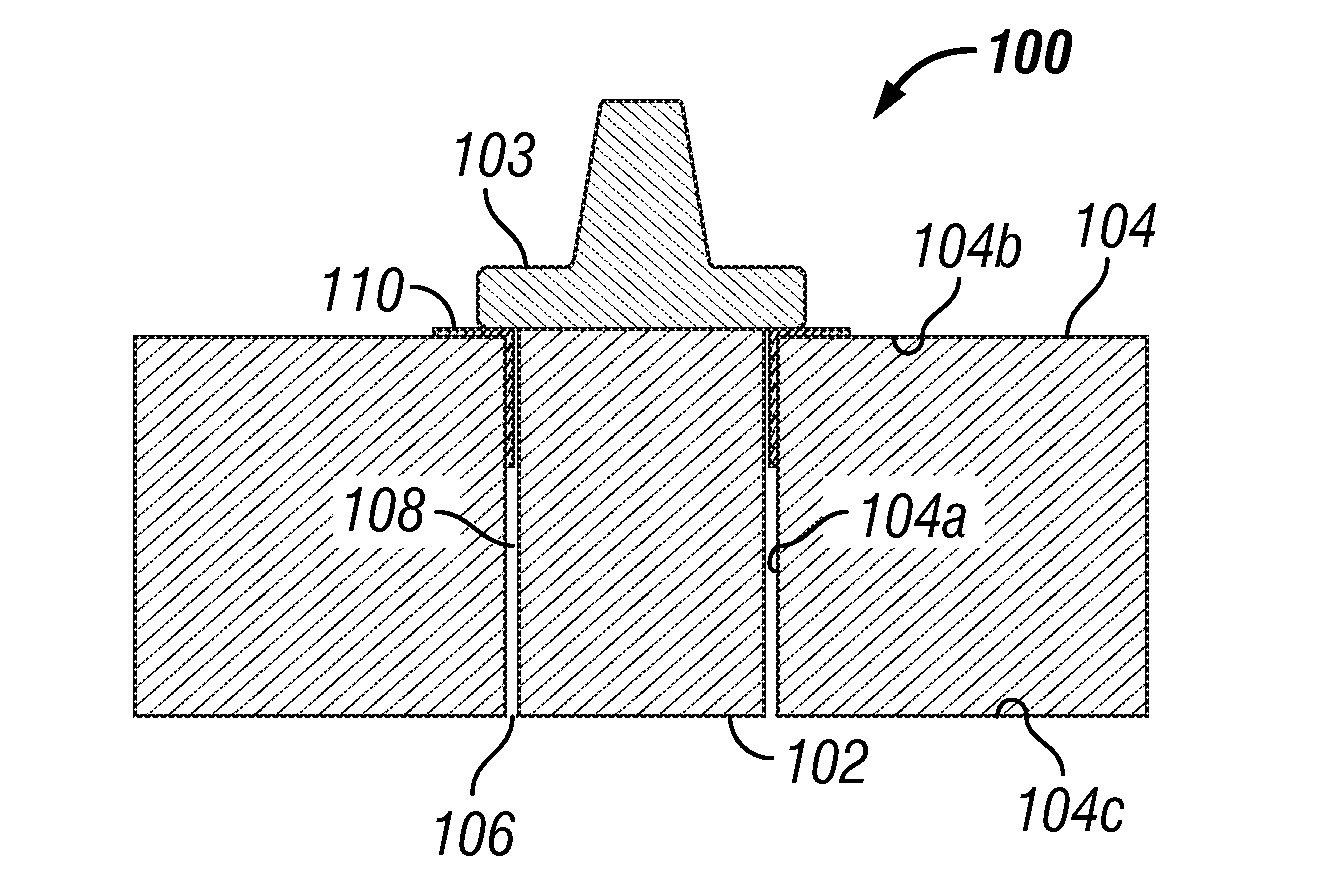
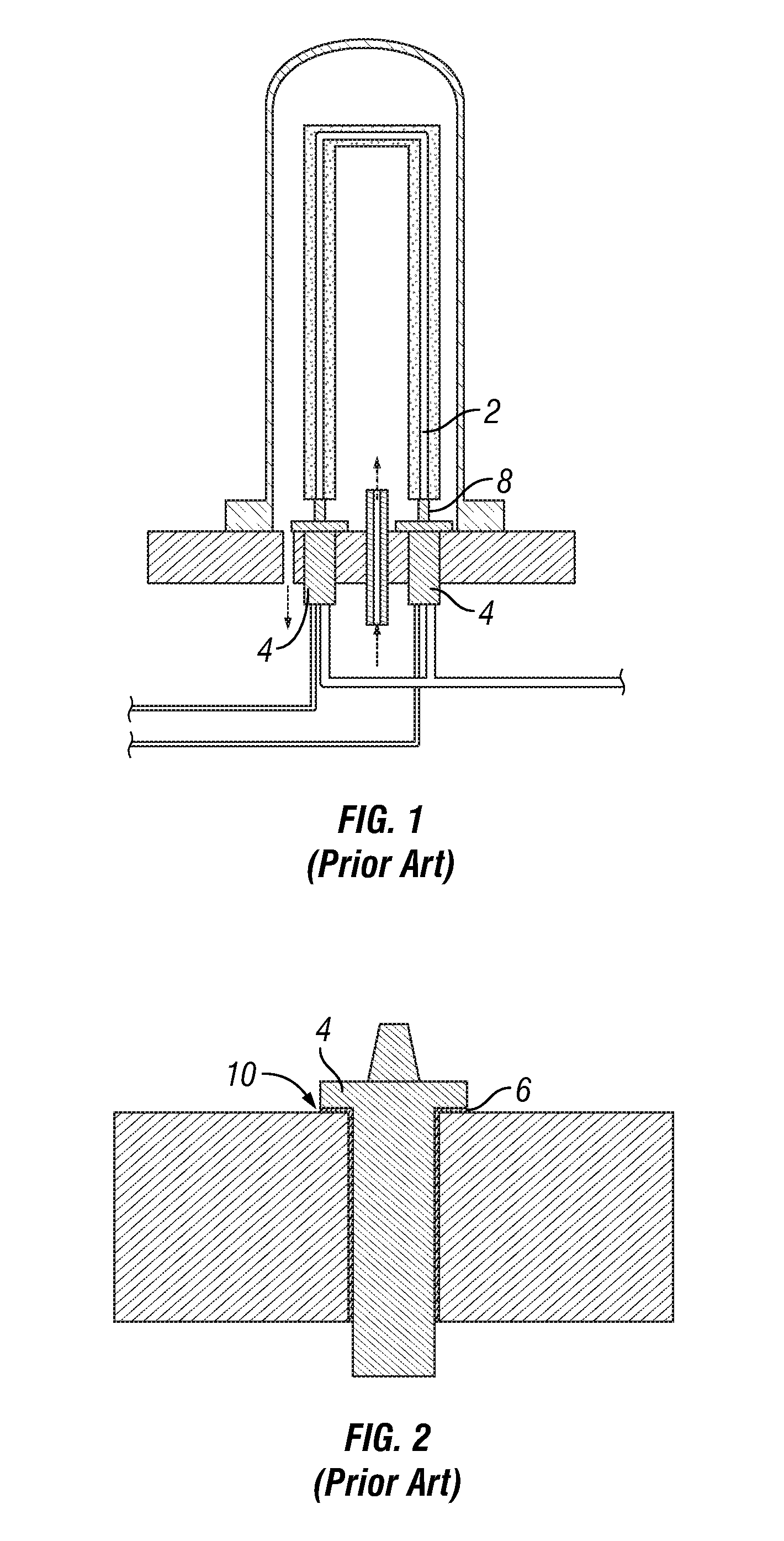
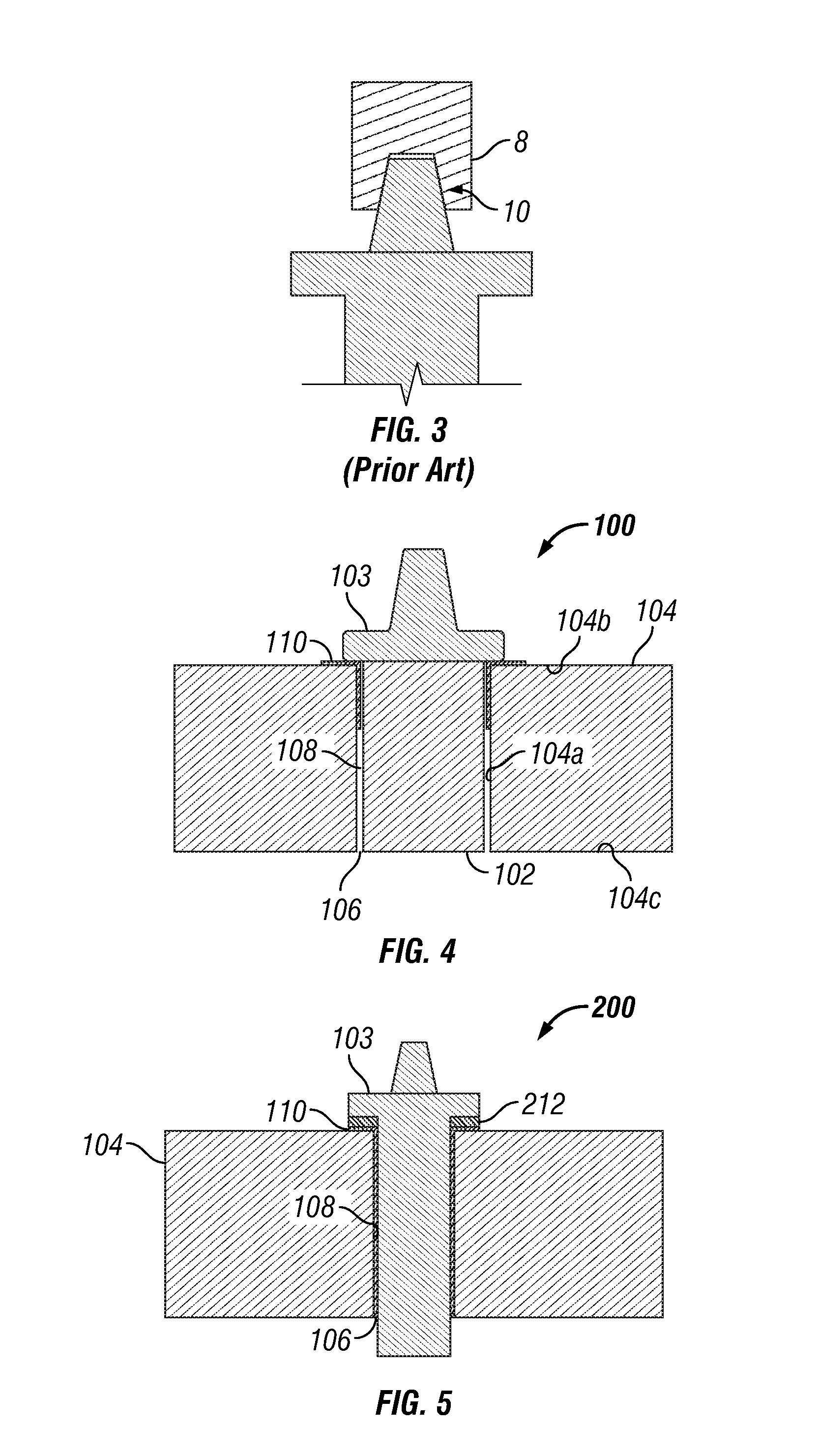
[0034]FIG. 4 illustrates an electrode 100, according to an embodiment of the present disclosure. The electrode 100 includes an electrode body 102 and a top electrode portion 103. The electrode 100 may be positioned through holes 104a in a base plate 104 of a chemical vapor deposition apparatus, such as the apparatus shown in FIG. 20 and described in greater detail below. Base plate 104 further includes an upper surface 104b and a bottom surface 104c.

[0035]An electrical isolation bushing 106 is positioned between the electrode 100 and the base plate 104. The electrical isolation bushing 106 includes a sleeve portion 108 surrounding a portion of the electrode body 102 that extends through the base plate 104. The electrical isolation bushing 106 also includes a collar portion 110 surrounding the holes 104a at the upper surface 104b of the base plate 104. In an embodiment, the collar portion 110 can be separable from the sleeve portion 108. The collar portion 110 can comprise a differe...


PUM

PropertyMeasurementUnit
Temperatureaaaaaaaaaa
Weightaaaaaaaaaa
Timeaaaaaaaaaa

Abstract

A chemical vapor deposition apparatus is disclosed. The chemical vapor deposition apparatus comprises a chamber having a base plate, a chamber wall, a gas inlet and a gas outlet. The base plate has holes therethrough. A plurality of electrodes extend through the holes of the base plate. The plurality of electrodes are capable of being attached to a power source. At least two of the plurality of electrodes are capable of being electrically coupled to a silicon rod positioned in the chamber. An electrical isolation bushing can be positioned between each of the plurality of electrodes and the base plate. The electrical isolation bushing comprises a sleeve portion surrounding a portion of the electrodes that extends through the base plate and a collar portion surrounding the holes at a surface of the base plate. In some instances, the collar portion can comprise a different material than the sleeve portion. In some instances, an isolation layer can be employed in addition to the isolation bushing, the isolation layer surrounding the holes at the surface of the base plate. In some instances, the collar portion and the sleeve portion are both ceramic.

Description

RELATED APPLICATIONS[0001]The present application claims benefit of U.S. Provisional Patent Application Nos. 61 / 122,066, filed on Dec. 12, 2008, and 61 / 164,552, filed on Mar. 30, 2009, both of which applications are incorporated herein by reference in their entirety. The present application further claims benefit of U.S. patent application Ser. No. 12 / 607,860, filed on Oct. 28, 2009, which claims benefit of U.S. Provisional Patent Application No. 61 / 109,137, filed on Oct. 28, 2008, both of which applications are incorporated herein by reference in their entirety.BACKGROUND[0002]1. Field of the Disclosure[0003]The present disclosure relates generally to electrodes, such as electrodes employed in CVD reactors.[0004]2. Description of the Related Art[0005]A popular method of manufacturing high purity polycrystalline silicon is through the use of a CVD reactor. FIG. 1 illustrates an example of a CVD reactor employed in such methods, which is known as a “Siemens Reactor”. During the manuf...

Claims


Application Information

Patent Timeline
IPC IPC(8): C23C16/00B23P6/00
CPCC01B33/035C23C16/509Y10T29/49718H01J37/32541H01J37/32559H01J37/32091
Inventor HSIEH, JUI HAIDELONG, DAVID
Owner GTSP GLOBAL
Why Eureka
Try Eureka