Semiconductor light-emitting device and method for manufacturing the same

a semiconductor and light-emitting device technology, applied in the direction of semiconductor/solid-state device manufacturing, semiconductor devices, electrical devices, etc., can solve the problems of reduced light-emitting intensity, reduced light-emitting efficiency as the entire semiconductor light-emitting device is reduced, and increased current density, so as to prevent the occurrence of migration with more certainty, reduce the light-emitting efficiency, and prevent the light-emitting effect of the second electrode from being decreased

Active Publication Date: 2010-06-17
SONY CORP
View PDF8 Cites 25 Cited by
  • Summary
  • Abstract
  • Description
  • Claims
  • Application Information

AI Technical Summary

Benefits of technology

[0007]Normally, part of light emitted in the active layer 23 is reflected between the laminated body and the substrate 10. When part of the reflected light reaches the upper layer protruding region, some of the part of the reflected light is absorbed at the upper layer 132 composed of nickel and constituting the upper layer protruding region and the reminder is reflected. As described above, the upper layer protruding region functions as a light-absorbing region, thereby posing a problem in that the light extraction efficiency as the entire semiconductor light-emitting device is reduced. Furthermore, an electric current is not injected into the laminated body exposed region from the second electrode 130, thereby posing a problem in that current density is increased at the light-emitting portion and thus the light-emitting intensity is decreased due to a luminance saturation phenomenon.
[0008]Typical values of D1 and D2 are 1 μm. Thus, in a large semiconductor light-emitting device including a projecting laminated body having a size of about 0.35 mm×0.35 mm, the total area of the laminated body exposed region and the upper layer protruding region is at most 2% of the area of the projecting laminated body. However, in a minute semiconductor light-emitting device including a projecting laminated body having a size of about 10 μm×10 μm, the total area of the laminated body exposed region and the upper layer protruding region accounts for as much as 64% of the area of the projecting laminated body. Therefore, the light reflecting effect produced by the lower layer 131 composed of silver (Ag) is decreased in such a minute semiconductor light-emitting device. Moreover, in such a minute semiconductor light-emitting device, the light extraction efficiency as the entire semiconductor light-emitting device is further reduced, and the light-emitting intensity is further decreased due to a luminance saturation phenomenon.
[0009]Accordingly, it is desirable to provide a semiconductor light-emitting device having a structure and a construction that can prevent the light reflecting effect of the second electrode from being decreased and can suppress the occurrence of migration without causing a decrease in the light extraction efficiency as the entire semiconductor light-emitting device and a decrease in the light-emitting intensity due to a luminance saturation phenomenon. It is also desirable to provide a method for manufacturing such a semiconductor light-emitting device.
[0038]In the present invention, the second electrode is formed on the transparent conductive material layer exposed at a bottom of the opening and on the insulating layer in a continuous manner and is not directly in contact with the light-emitting portion. Thus, the migration of a material (atoms) constituting the second electrode to the light-emitting portion can be prevented with certainty. In addition, since S2<S3 is satisfied, the occurrence of migration can be prevented with more certainty as described below. Since S2<S4 is satisfied, the light reflecting effect of the second electrode can be certainly prevented from being decreased. Furthermore, the satisfaction of S1 S2 does not cause a decrease in the light extraction efficiency as the entire semiconductor light-emitting device and a decrease in the light-emitting intensity due to a luminance saturation phenomenon. If the value of S3 / S2 or S4 / S2 is decreased to the limitation of alignment precision in manufacturing, the size as the entire semiconductor light-emitting device can be decreased to its limitation and semiconductor light-emitting devices can be formed at a narrower pitch even if the active layer has the same area. Consequently, a larger number of semiconductor light-emitting devices can be obtained from a single crystal growth substrate. Accordingly, the manufacturing cost of the semiconductor light-emitting device can be reduced.

Problems solved by technology

As described above, the upper layer protruding region functions as a light-absorbing region, thereby posing a problem in that the light extraction efficiency as the entire semiconductor light-emitting device is reduced.
Furthermore, an electric current is not injected into the laminated body exposed region from the second electrode 130, thereby posing a problem in that current density is increased at the light-emitting portion and thus the light-emitting intensity is decreased due to a luminance saturation phenomenon.

Method used


Image

  • Semiconductor light-emitting device and method for manufacturing the same
  • Semiconductor light-emitting device and method for manufacturing the same
  • Semiconductor light-emitting device and method for manufacturing the same

Examples


example 1

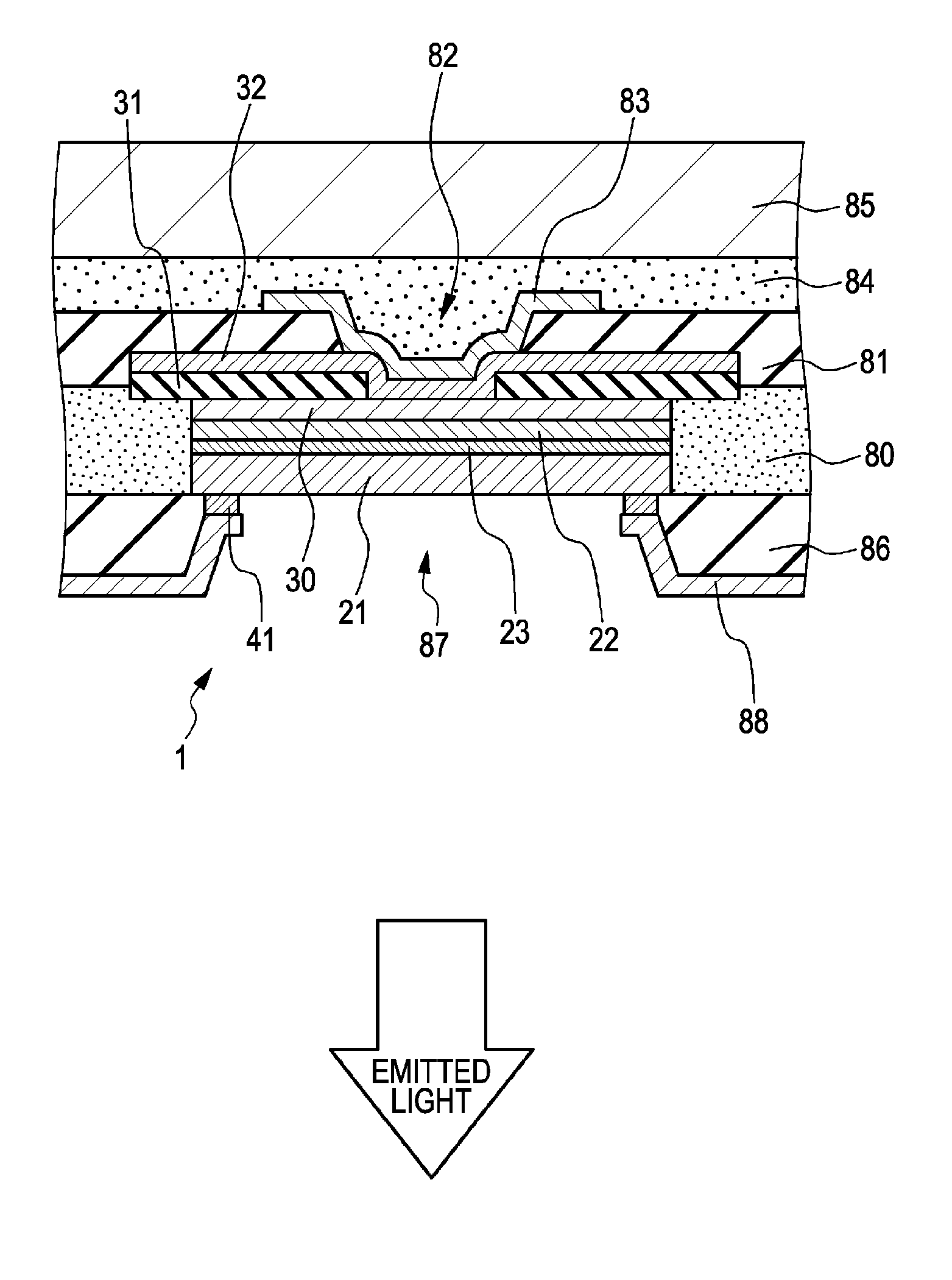
[0050]Example 1 relates to a semiconductor light-emitting device according to an embodiment of the present invention and a method for manufacturing the semiconductor light-emitting device. A semiconductor light-emitting device 1 in Example 1 is specifically composed of a light-emitting diode.

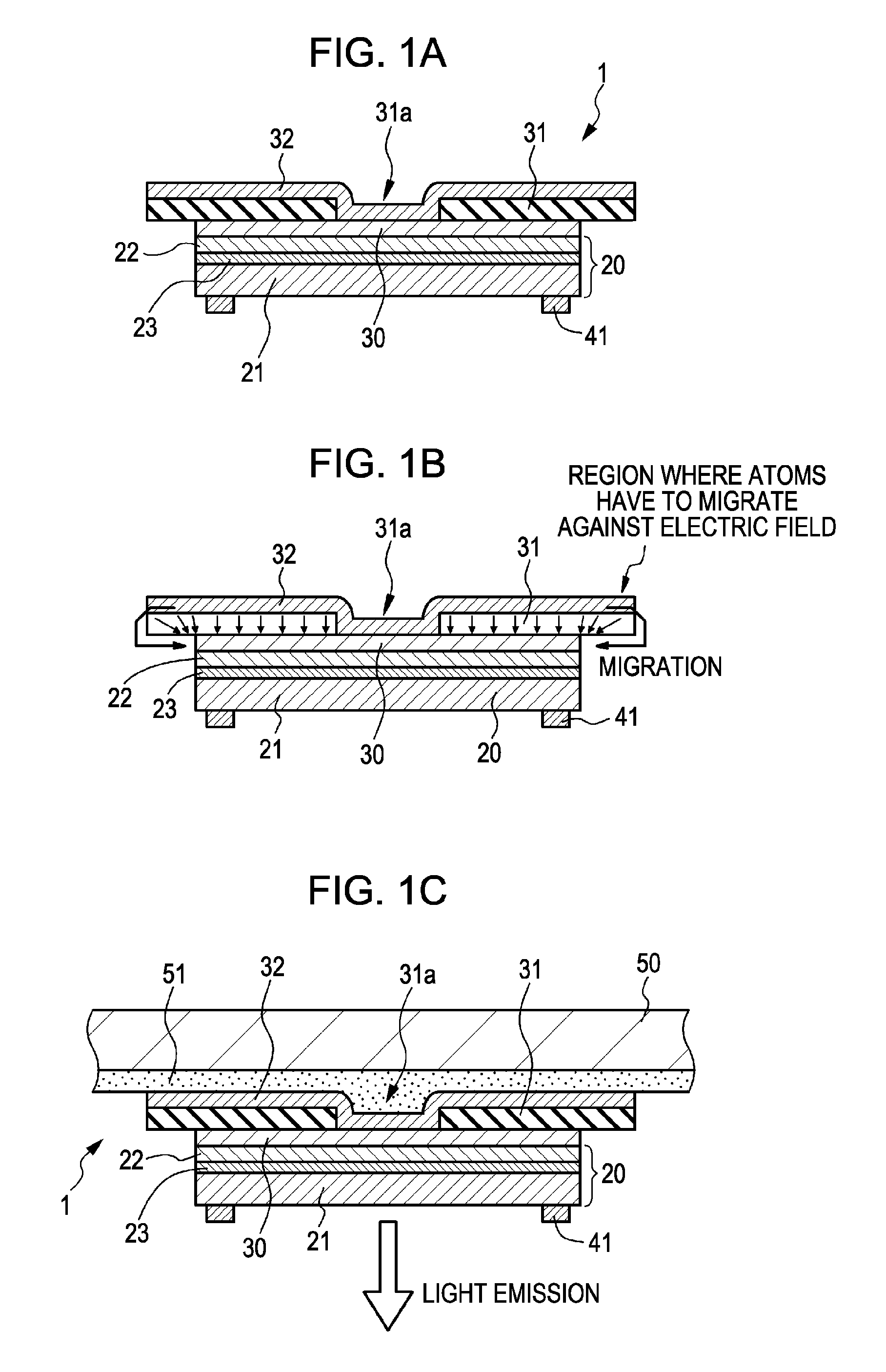
[0051]As shown in FIG. 1A that is a conceptual diagram and FIG. 1C that is a schematic sectional view, the semiconductor light-emitting device 1 of Example 1 includes:

[0052](A) a light-emitting portion 20 obtained by laminating in sequence a first compound semiconductor layer 21 having a first conductivity type (specifically, n type in Example 1), an active layer 23, and a second compound semiconductor layer 22 having a second conductivity type (specifically, p type in Example 1) that is different from the first conductivity type;

[0053](B) a first electrode (n-side electrode) 41 electrically connected to the first compound semiconductor layer 21;

[0054](C) a transparent conductive material layer ...

example 2

[0091]Example 2 is a modification of Example 1. In Example 2, the semiconductor light-emitting devices 1 obtained in Example 1 are rearranged in an array (in a two-dimensional matrix) to manufacture, for example, an image display apparatus. Specifically, in Example 2, the steps described below are performed after Step-160.

[0092]Step-200

[0093]In this step, semiconductor light-emitting devices 1 are selected at a desired pitch. More specifically, semiconductor light-emitting devices 1 are selected from many semiconductor light-emitting devices 1 that are obtained in Step-160 of Example 1 and are arranged in a two-dimensional matrix, at a pitch of every M devices in an X direction and every N devices in a Y direction. There are prepared a relay substrate 60 on which a weak adhesive layer 61 composed of silicone rubber is formed and a second relay substrate 70 in which an alignment mark (not shown) composed of a metal thin film or the like is formed in a predetermined position and on wh...


PUM


Abstract

A semiconductor light-emitting device includes (A) a light-emitting portion obtained by laminating in sequence a first compound semiconductor layer, an active layer, and a second compound semiconductor layer; (B) a first electrode electrically connected to the first compound semiconductor layer; (C) a transparent conductive material layer formed on the second compound semiconductor layer; (D) an insulating layer composed of a transparent insulating material and having an opening, the insulating layer being formed on the transparent conductive material layer; and (E) a second electrode that reflects light from the light-emitting portion, the second electrode being formed on the transparent conductive material layer and on the insulating layer in a continuous manner, wherein, assuming that areas of the active layer, the transparent conductive material layer, the insulating layer, and the second electrode are respectively S1, S2, S3, and S4, S1≦S2<S3 and S2<S4 are satisfied.

Description

BACKGROUND OF THE INVENTION[0001]1. Field of the Invention[0002]The present invention relates to a semiconductor light-emitting device and a method for manufacturing the semiconductor light-emitting device.[0003]2. Description of the Related Art[0004]Semiconductor light-emitting devices such as light-emitting diodes (LEDs), for example, include a light-emitting portion 20 composed of a projecting laminated body obtained by laminating an n conductivity type first compound semiconductor layer 21, an active layer 23, and a p conductivity type second compound semiconductor layer 22 in sequence on a semiconductor light-emitting device manufacturing substrate (hereinafter may be simply referred to as a substrate 10). A first electrode (n-side electrode) 41 is disposed on the substrate 10 or an exposed portion 21a of the exposed first compound semiconductor layer 21. A second electrode (p-side electrode) 130 is disposed on the top face of the second compound semiconductor layer 22. Such se...

Claims


Application Information

Patent Timeline
Patent Type & Authority Applications(United States)
IPC IPC(8): H01L33/00H01L21/28
CPCH01L33/38H01L33/44H01L33/486H01L2933/0016H01L2924/0002H01L2924/00
Inventor TOMODA, KATSUHIRO
Owner SONY CORP
Why Eureka
Try Eureka