Metal oxide semiconductor device

Active Publication Date: 2010-06-17
UNITED MICROELECTRONICS CORP
View PDF5 Cites 44 Cited by
  • Summary
  • Abstract
  • Description
  • Claims
  • Application Information

AI Technical Summary

Benefits of technology

[0008]Accordingly, at least one objective of the present invention is to provide a metal oxide semiconductor (MOS) device, applicable for the driver ICs of the LCD panels, that affords lower elec

Problems solved by technology

However, as the size of the LCD panels keeps increasin

Method used


Image

  • Metal oxide semiconductor device
  • Metal oxide semiconductor device
  • Metal oxide semiconductor device

Examples


Embodiment Construction

[0024]Reference will now be made in detail to the present preferred embodiments of the invention, examples of which are illustrated in the accompanying drawings. Wherever possible, the same reference numbers are used in the drawings and the description to refer to the same or like parts.

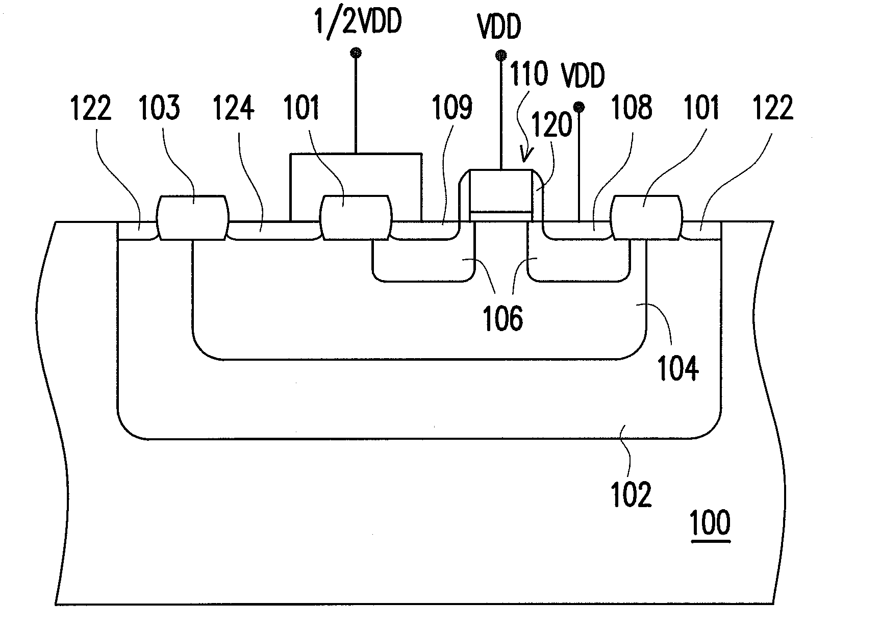
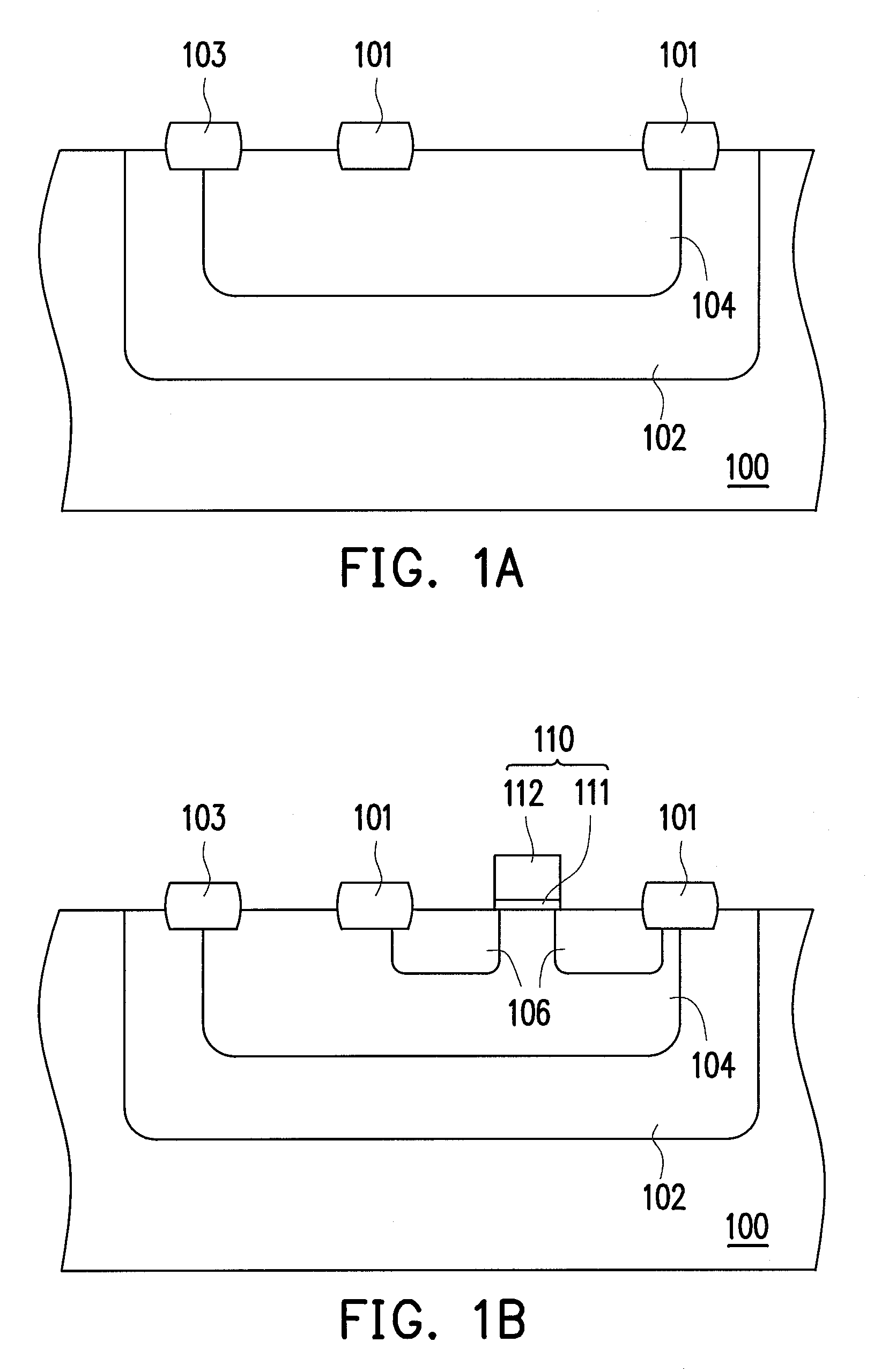
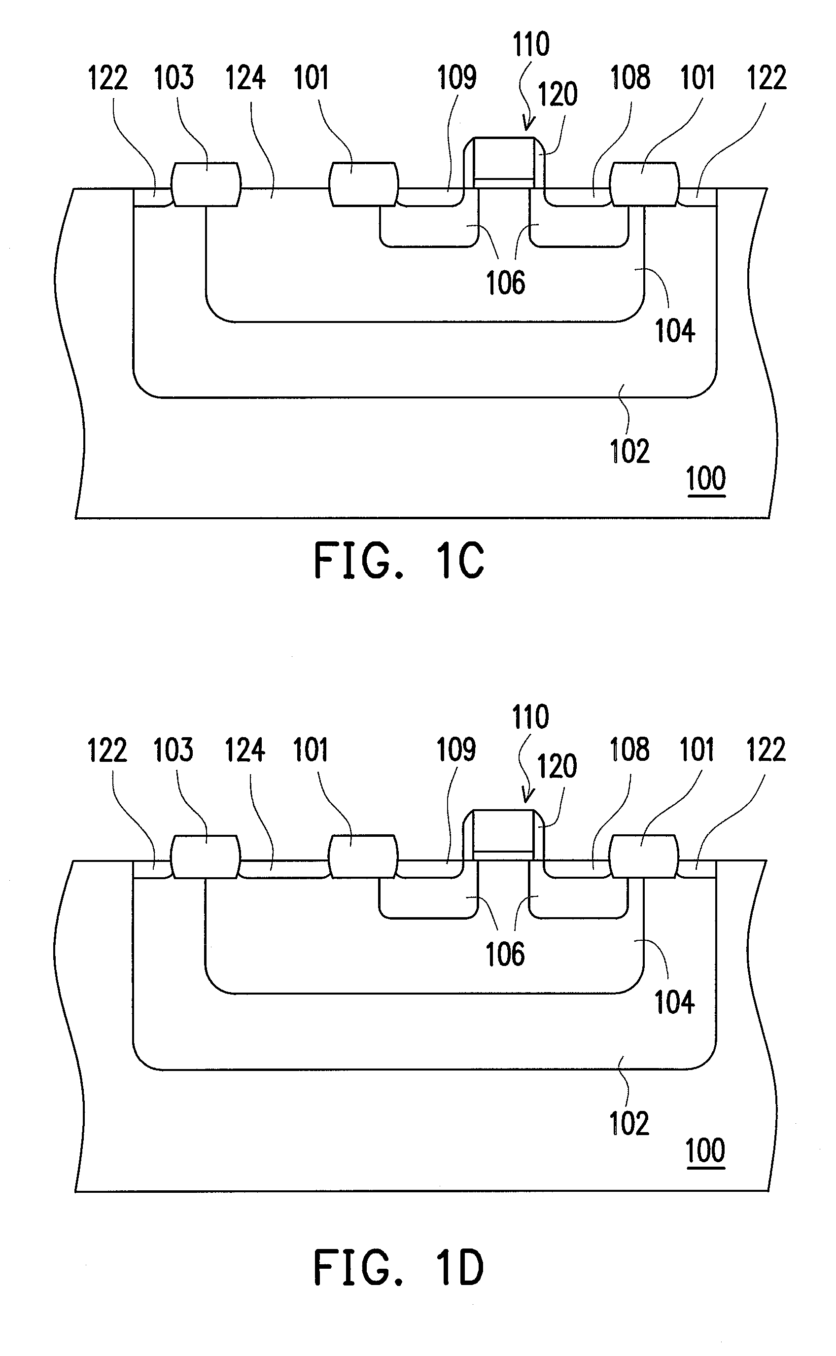
[0025]FIGS. 1A through 1D are schematic cross-sectional views showing the steps for fabricating a MOS transistor device according to one preferred embodiment of the present invention. As shown in FIG. 1A, a substrate 100 is provided. The substrate 100 is a P-type silicon substrate, for example. Then, an N-type deep well 102 is formed in the substrate 100. The method of forming the N-type deep well 102 includes performing an ion implant process using phosphorus as the dopants, for example. Thereafter, a P-type well 104 is formed in the N-type deep well 102 such that the N-type deep well 102 surrounds the P-well 104. The P-type well 104 is formed, for example, by performing an ion implant using boron a...


PUM


Abstract

A metal oxide semiconductor device comprising a substrate, at least an isolation structure, a deep N-type well, a P-type well, a gate, a plurality of N-type extension regions, an N-type drain region, an N-type source region and a P-type doped region is provided. The N-type extension regions are disposed in the substrate between the isolation structures and either side of the gate, while the N-type drain region and the N-type source region are respectively disposed in the N-type extension regions at both sides of the gate. The P-type well surrounds the N-type extension regions, and the P-type doped region is disposed in the P-type well of the substrate and is isolated from the N-type source region by the isolation structure.

Description

BACKGROUND OF THE INVENTION[0001]1. Field of the Invention[0002]The present invention relates to a semiconductor device. More particularly, the present invention relates to a metal oxide semiconductor (MOS) device.[0003]2. Description of the Related Art[0004]Liquid crystal display (LCD) has become the main stream of the display apparatuses. Due to its advantages of light-weight, compact, applicable in various sizes and low radiation, the LCD is suitably used as the display screen for portable electronic apparatuses such as the notebooks, the mobile phones and global positioning systems (GPS) etc.[0005]Owing to the limited power capacity of the battery, it is desirable for the LCDs used in the portable electronic apparatuses to offer lower electricity consumption. However, as the size of the LCD panels keeps increasing, the electricity consumption is inevitably increased.[0006]In general, high voltage devices are widely used in the driver integrated circuits (ICs) of the LCD panels a...

Claims


Application Information

Patent Timeline
IPC IPC(8): H01L29/78
CPCH01L21/761H01L29/7833H01L21/823892H01L21/823493
Inventor LIN, SHIN-KUANGWANG, LUNG-CHIHHUANG, CHUNG-MINGYANG, CHE-CHINGCHEN, CHUN-MING
Owner UNITED MICROELECTRONICS CORP
Why Eureka
Try Eureka