Soi radio frequency switch for reducing high frequency harmonics

a radio frequency switch and harmonic reduction technology, applied in the field of semiconductor structures, can solve problems such as reducing the effectiveness of rf switches

Active Publication Date: 2010-06-24
GLOBALFOUNDRIES US INC
View PDF10 Cites 22 Cited by
  • Summary
  • Abstract
  • Description
  • Claims
  • Application Information

AI Technical Summary

Benefits of technology

[0008]According to an aspect of the present invention, a method of forming a semiconductor structure is provided, which includes: forming at least one field effect transistor on a top semiconductor layer of a semiconductor-on-insulator (SOI) substrate including a bottom semiconductor layer having a doping of a first conductivity type; forming a shallow trench isolation structure in the top semiconductor layer, wherein the shallow trench isolation structure laterally abuts and surrounds the at least one field effect transistor; forming a first doped semiconductor region in the bottom semiconductor layer, wherein the first doped semiconductor region abuts the buried insulator layer and has a doping of the first conductivity type; and forming a second doped semiconductor region in the bottom semiconductor layer, wherein the second doped semiconductor region abuts the buried insulator layer and has a doping of the first conductivity type, wherein the second conductivity type is the opposite of the first conductivity type, and wherein the first and second doped semiconductor region are electrically connected through at least one metal interconnect structure located above the SOI substrate.
[0009]According to another aspect of the present invention, a method of operating a semiconductor device is provided. The method of operation includes: providing a semiconductor device containing: a semiconductor-on-insulator (SOI) substrate including a top semiconductor layer, a buried insulator layer, and a bottom semiconductor layer having a doping of a first conductivity type; at least one field effect transistor located on the top semiconductor layer; a shallow trench isolation structure laterally abutting the at least one field effect transistor; a first doped semiconductor region embedded in the bottom semiconductor layer and abutting the buried insulator layer and having a doping of the first conductivity type; and a second doped semiconductor region embedded in the bottom semiconductor layer and abutting the buried insulator layer and having a doping of a second conductivity type, wherein the second conductivity type is the opposite of the first conductivity type; applying a radio frequency (RF) signal to the at least one field effect transistor, wherein an induced charge layer is formed directly underneath the buried insulator layer; and electrically biasing the first and second doped semiconductor regions at a same voltage.
[0010]According to yet another aspect of the present invention, a semiconductor structure is provided. The semiconductor structure includes: a semiconductor-on-insulator (SOI) substrate including a top semiconductor layer, a buried insulator layer, and a bottom semiconductor layer having a doping of a first conductivity type; at least one field effect transistor located on the top semiconductor layer; a shallow trench isolation structure laterally abutting the at least one field effect transistor; a first doped semiconductor region embedded in the bottom semiconductor layer and abutting the buried insulator layer and having a doping of the first conductivity type; and a second doped semiconductor region embedded in the bottom semiconductor layer and abutting the buried insulator layer and having a doping of a second conductivity type, wherein the second conductivity type is the opposite of the first conductivity type, and wherein the first and second doped semiconductor region are electrically biased at a same voltage.
[0011]According to still another aspect of the present invention, a design structure embodied in a machine readable medium for designing, manufacturing, or testing a design for a semiconductor structure is provided. The design structure includes: a first data representing a semiconductor-on-insulator (SOI) substrate including a top semiconductor layer, a buried insulator layer, and a bottom semiconductor layer having a doping of a first conductivity type; a second data representing at least one field effect transistor located on the top semiconductor layer; a third data representing a shallow trench isolation structure laterally abutting the at least one field effect transistor; a fourth data representing a first doped semiconductor region embedded in the bottom semiconductor layer and abutting the buried insulator layer and having a doping of the first conductivity type; and a fifth data representing a second doped semiconductor region embedded in the bottom semiconductor layer and abutting the buried insulator layer and having a doping of a second conductivity type, wherein the second conductivity type is the opposite of the first conductivity type, wherein the first and second doped semiconductor region are electrically biased at a same voltage.

Problems solved by technology

The spurious capacitive coupling between the induced charge layer in the bottom semiconductor layer and the other semiconductor devices provides a secondary capacitive coupling, which is a parasitic coupling that reduces the effectiveness of the RF switch.

Method used


Image

  • Soi radio frequency switch for reducing high frequency harmonics
  • Soi radio frequency switch for reducing high frequency harmonics
  • Soi radio frequency switch for reducing high frequency harmonics

Examples


Embodiment Construction

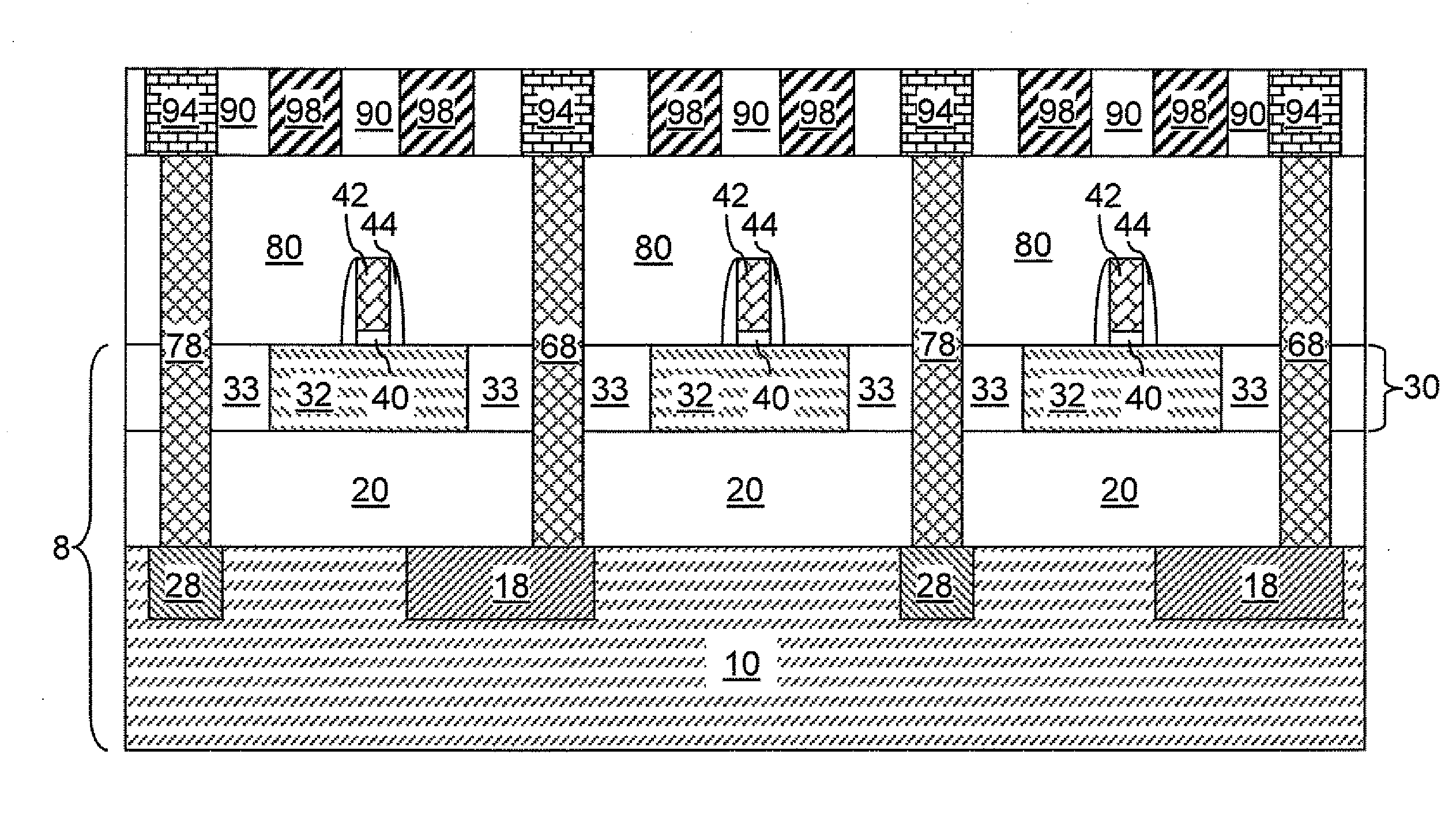
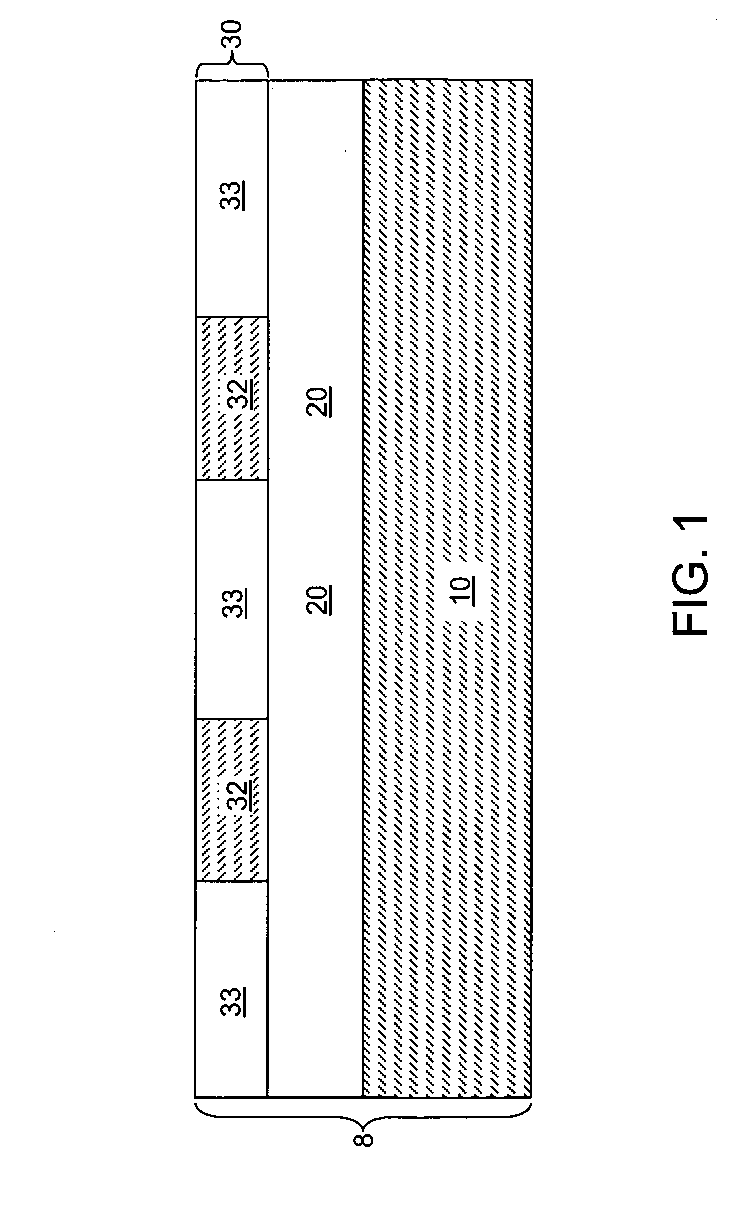
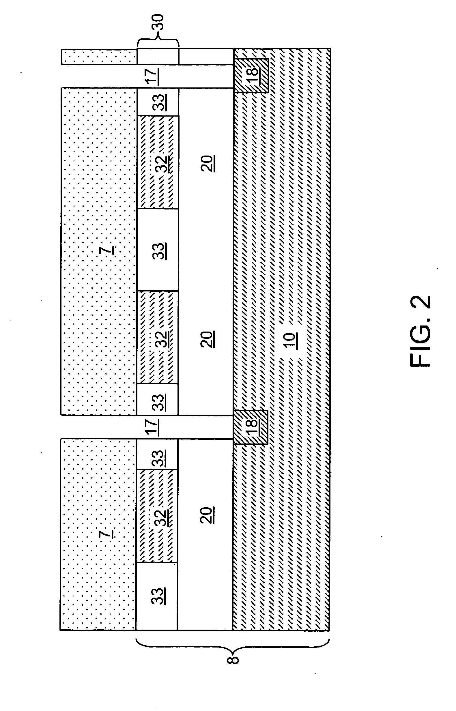
[0019]As stated above, the present invention relates to a semiconductor structure including a radio frequency switch on a semiconductor-on-insulator (SOI) substrate, methods of manufacturing the same, and methods of operating the same, which are described herein with accompanying figures. The drawings are not necessarily drawn to scale.

[0020]As used herein, radio frequency (RF) denotes a frequency of electromagnetic wave within the range of 3 Hz to 300 GHz. Radio frequency corresponds to the frequency of electromagnetic wave that is used to produce and detect radio waves. Radio frequency includes very high frequency (VHF), ultra high frequency (UHF), super high frequency (SHF), and extremely high frequency (EHF).

[0021]As used herein, very high frequency (VHF) refers to a frequency in the range from 30 MHz to 300 MHz. VHF is used, among others, for frequency modulation (FM) broadcasting. Ultra high frequency (UHF) refers to a frequency in the range from 300 MHz to 3 GHz. UHF is used,...


PUM


Abstract

First doped semiconductor regions having the same type doping as a bottom semiconductor layer and second doped semiconductor regions having an opposite type doping are formed directly underneath a buried insulator layer of a semiconductor-on-insulator (SOI) substrate. The first doped semiconductor regions and the second doped semiconductor regions are electrically grounded or forward-biased relative to the bottom semiconductor layer at a voltage that is insufficient to cause excessive current due to forward-biased injection of minority carriers into the bottom semiconductor layer, i.e., at a potential difference not exceeding 0.6 V to 0.8V. The electrical charges formed in an induced charge layer by the electrical signal in semiconductor devices on the top semiconductor layer are drained through electrical contacts connected to the first and second doped semiconductor regions, thereby reducing of harmonic signals in the semiconductor devices above and enhancing the performance of the semiconductor devices as a radio-frequency (RF) switch.

Description

FIELD OF THE INVENTION[0001]The present invention relates to semiconductor structures, and particularly to a semiconductor structure including a radio frequency switch on a semiconductor-on-insulator (SOI) substrate, methods of manufacturing the same, and methods of operating the same.BACKGROUND OF THE INVENTION[0002]Semiconductor devices such as field effect transistors are employed as a switching device for radio frequency (RF) signals in analog and RF applications. Semiconductor-on-insulator (SOI) substrates are typically employed for such applications since parasitic coupling between devices through the substrate is reduced due to the low dielectric constant of a buried insulator layer. For example, the dielectric constant of silicon, which comprises the entirety of the substrate of a bulk silicon substrate, is 11.7 in gigahertz ranges. In contrast, the dielectric constant of silicon oxide, which isolates a top semiconductor layer containing devices from a handle substrate, is 3...

Claims


Application Information

Patent Timeline
Patent Type & Authority Applications(United States)
IPC IPC(8): H01L21/265H03K3/01H01L29/786G06F17/50
CPCH01L21/76224H01L27/1203H01L21/84H01L21/76251H01L21/18H01L21/20H01L27/02
Inventor BOTULA, ALAN B.NOWAK, EDWARD J.SLINKMAN, JAMES A.
Owner GLOBALFOUNDRIES US INC
Why Eureka
Try Eureka