Lens array device and image display

an array device and array technology, applied in optics, instruments, electrical devices, etc., can solve the problems of very etc., and achieve poor image display quality in the two-dimensional display mode, disadvantageous in power consumption, and disadvantageous in process and cos

Inactive Publication Date: 2010-06-24
SONY CORP
View PDF4 Cites 77 Cited by
  • Summary
  • Abstract
  • Description
  • Claims
  • Application Information

AI Technical Summary

Benefits of technology

[0018]On the other hand, in the case where the lens array illustrated in FIGS. 17A and 17B is used, a state in which a voltage is not applied to the liquid crystal layer 103 is a state with no lens effect, that is, the two-dimensional display mode. Therefore, in the case where the two-dimensional display mode is frequently used, it is advantageous in power consumption. Moreover, a lens-shaped mold is not included in the liquid crystal layer 103, so compared to the lens array illustrated in FIGS. 15 and 16, image display quality in the two-dimensional display mode is less prone to degradation.
[0025]In the image display according to the embodiment of the invention, for example, appropriate switching the state in the lens array device between the state with no lens effect and the first lens state or the second lens state allows electrical switching between two-dimensional display and three-dimensional display to be achieved. For example, putting the lens array device into the state with no lens effect allows display image light from the display panel to pass through the lens array device without any deflection, thereby to achieve two-dimensional display. Moreover, putting the lens array device into the first lens state allows the display image light from the display panel to be deflected in a direction orthogonal to the first direction, thereby to achieve three-dimensional display where a stereoscopic effect is obtained when both eyes of a viewer are placed along a direction orthogonal to the first direction. Further, putting the lens array device into the second lens state allows the display image light from the display panel to be deflected in a direction orthogonal to the second direction, thereby to achieve three-dimensional display where a stereoscopic effect is obtained when both eyes of the viewer are placed along a direction orthogonal to the second direction.
[0026]In the lens array device according to the embodiment of the invention, the first electrode group and the second electrode group are arranged so as to face each other with the liquid crystal layer in between, and the first electrode group and the second electrode group each include a plurality of transparent electrodes extending in two different directions, and the state of voltages applied to the first electrode group and the second electrode group is appropriately controlled so as to appropriately control a lens effect in the liquid crystal layer, so electrical switching between the presence and absence of the lens effect is easily allowed. Moreover, the lens effect of a cylindrical lens is easily electrically switchable between two directions.
[0027]In the image display according to the embodiment of the invention, as an optical device selectively changing the transmission state of a light ray from the display panel, the lens array device according to the embodiment of the invention is used, so, for example, electrical switching between two-dimensional display and three-dimensional display is easily allowed to be achieved. Moreover, for example, the display direction in the case where three-dimensional display is achieved is electrically easily switchable between two different directions.

Problems solved by technology

However, in the case where the lens array illustrated in FIGS. 15 and 16 is used for switching between the two-dimensional display mode and the three-dimensional display mode, the following issues arise.
First, it is necessary to form a mold to be filled with the liquid crystal molecules 231 on a substrate, and forming the mold is very disadvantageous in process and cost.
Moreover, a state in which a lens effect is produced in the case where a voltage is not applied to the liquid crystal layer 223 is the three-dimensional display mode, but it is easily predicted that the two-dimensional display mode is more frequently used at present, so it is considered that it is disadvantageous in power consumption.
Further, image display quality in the two-dimensional display mode is poor, because of a specific mold included in the liquid crystal layer 223 or viewing angle dependence of a liquid crystal.
For example, in the case where the cylindrical lens array is arranged so that three-dimensional display is properly achieved in the landscape orientation display state, in the portrait orientation display state, refractive power is provided in a vertical direction, but refractive power is not provided in a lateral direction, so it is difficult to properly achieve stereoscopic vision.
Also in the case where a cylindrical lens array configured of liquid crystal lenses in related art is used, the same issue arises.
More specifically, in related art, switching between the two-dimensional display mode and the three-dimensional display mode is allowed through the use of the liquid crystal lenses, but in the three-dimensional display mode, it is difficult to achieve appropriate display switching in response to switching between the landscape orientation display state and the portrait orientation display state.
Moreover, in the case where like the liquid crystal lens described in Japanese Unexamined Patent Application Publication No. 2008-9370, a two-layer electrode configuration is formed on one side of the liquid crystal layer, it is necessary to arrange two layers including electrodes, and it is extremely disadvantageous in process and cost.
In other words, this state is the same as a state in which a thick alignment film is provided on the top substrate, and it is obvious that this state causes issues such as leading a burn-in phenomenon in a liquid crystal.

Method used


Image

  • Lens array device and image display
  • Lens array device and image display
  • Lens array device and image display

Examples


first embodiment

Whole Configurations of Lens Array Device and Image Display

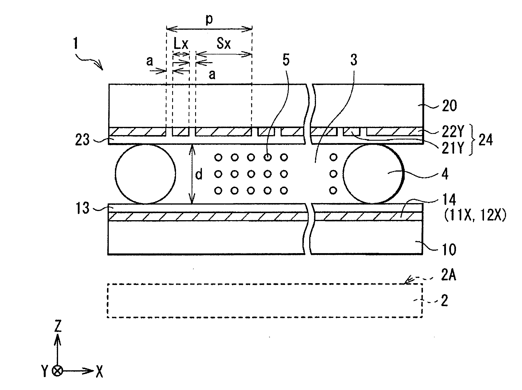
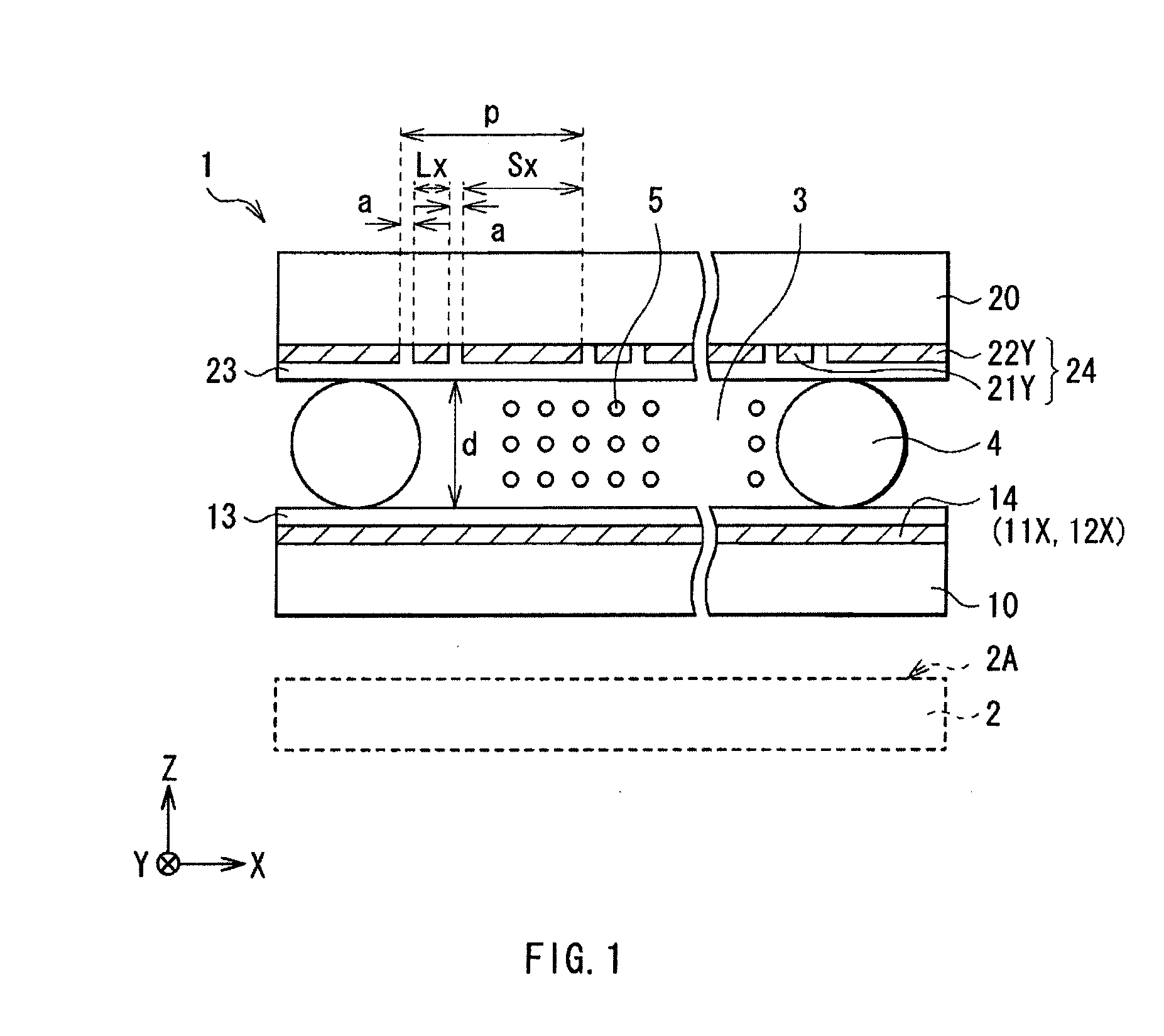
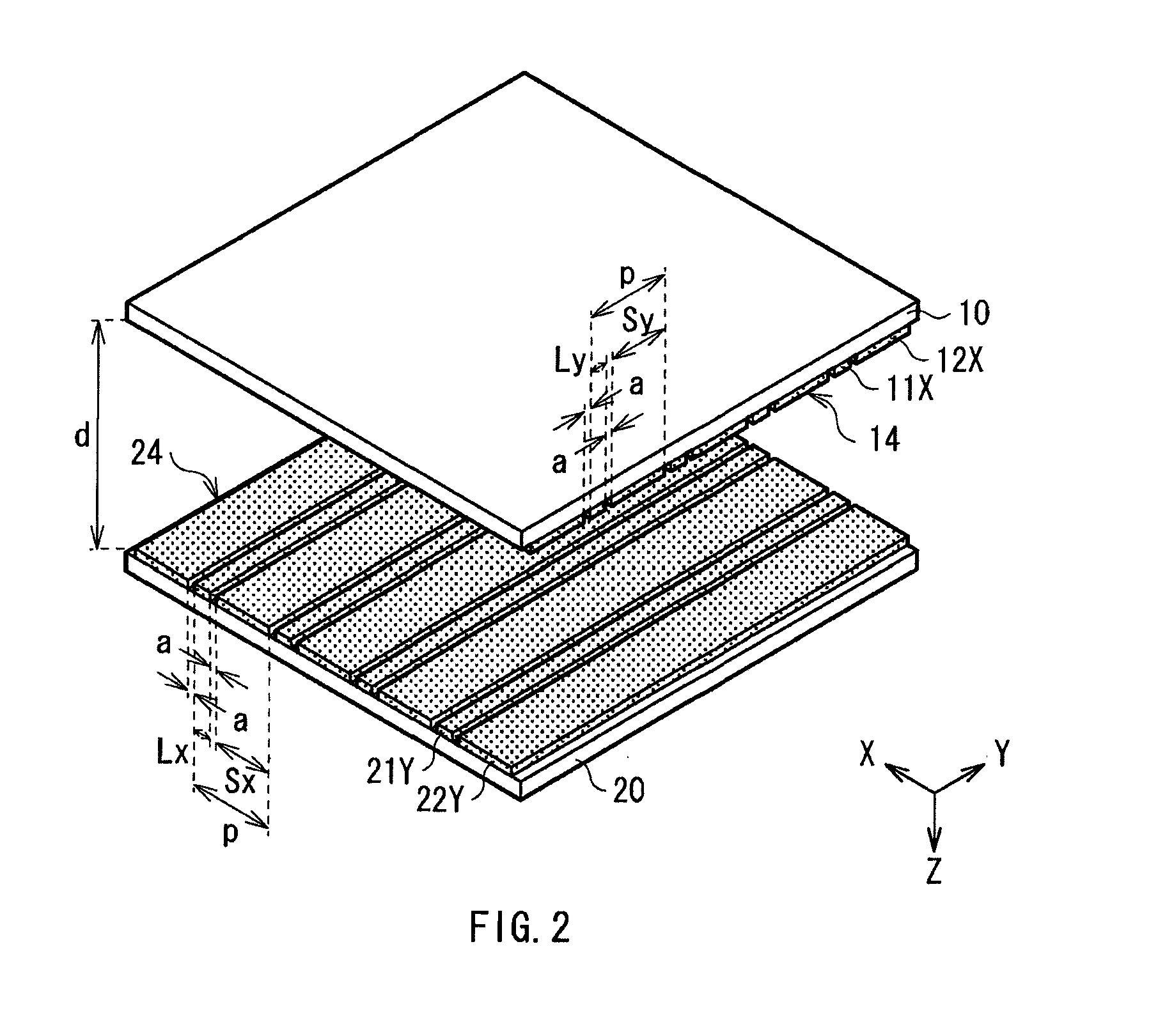
[0049]FIG. 1 illustrates a configuration example of a lens array device 1 according to a first embodiment of the invention. The lens array device 1 includes a first substrate 10 and a second substrate 20 which face each other with a distance d in between, and a liquid crystal layer 3 arranged between the first substrate 10 and the second substrate 20. The first substrate 10 and the second substrate 20 are transparent substrates made of, for example, a glass material or a resin material. A first electrode group 14 in which a plurality of transparent electrodes extending in a first direction are arranged in parallel at intervals in a width direction is formed on a side facing the second substrate 20 of the first substrate 10. An alignment film 13 is formed on the first substrate 10 with the first electrode group 14 in between. A second electrode group 24 in which a plurality of transparent electrodes extending in a second dire...

second embodiment

[0073]Next, a lens array device and an image display according to a second embodiment of the invention will be described below. Like components are denoted by like numerals as of the lens array device 1 and the image display according to the first embodiment, and will not be further described.

[0074]In the lens array device 1 according to the first embodiment, in the case where the application states of the drive voltage to the transparent electrodes on an upper side and a lower side are implemented by a driving method illustrated in FIG. 3, there is a possibility that a lens shape (the alignment state of the liquid crystal molecules 5) is changed with time, thereby not to control the liquid crystal layer 3 into a desired lens state. In particular, in the case where a gap between electrodes (the distance d between substrates) is narrowed so as to achieve higher definition and higher response speed and the like, there is a high possibility that the liquid crystal layer 3 is not contro...

examples

[0081]Next, specific examples of the image display using the lens array device 1 according to the embodiment will be described below.

[0082]FIG. 11 illustrates a configuration of an image display according to examples. In the example, as the first substrate 10 and the second substrate 20 of the lens array device 1, electrode substrates formed by arranging transparent electrodes made of ITO on glass substrates were used. Then, by a known photolithography method and a wet etching method or a dry etching method, the electrodes are patterned into shapes of electrodes of the first electrode group 14 (the first electrodes 11X and the second electrodes 12X) and the second electrode group 24 (the first electrodes 21Y and the second electrodes 22Y). Polyimide was applied to the substrates by spin coating, and then polyimide was fired to form the alignment films 13 and 23. After firing the material, a rubbing process was performed on surfaces of the alignment films 13 and 23, and the alignment...


PUM

PropertyMeasurementUnit
applied voltageaaaaaaaaaa
refractive index distributionaaaaaaaaaa
distanceaaaaaaaaaa

Abstract

The lens array device includes: first and second substrates; a first electrode group formed on the first substrate to include transparent electrodes extending in a first direction; a second electrode group formed on the second substrate to include transparent electrodes extending in a second direction; and a liquid crystal layer with refractive index anisotropy arranged between the first and second substrates to produce a lens effect by changing the liquid crystal molecule alignment. The liquid crystal layer electrically changes into one of three states according to voltages applied to the first and second electrode groups. The three states include a state with no lens effect, a first lens state where a lens effect of a first cylindrical lens extending in the first direction is produced, and a second lens state where a lens effect of a second cylindrical lens extending in the second direction is produced.

Description

[0001]The present application claims priority to Japanese Patent Application JP 2008-326503 filed in the Japanese Patent Office on Dec. 22, 2008 and Japanese Priority Patent Application JP 2009-063276 filed in the Japanese Patent Office on Mar. 16, 2009, the entire contents of which is hereby incorporated by reference.BACKGROUND OF THE INVENTION[0002]1. Field of the Invention[0003]The present invention relates to a lens array device allowed to electrically control the production of a lens effect through the use of a liquid crystal, and an image display which is electrically switchable between, for example, two-dimensional display and three-dimensional display through the use of the lens array device.[0004]2. Description of the Related Art[0005]In related art, a binocular or multi-ocular stereoscopic display which achieves stereoscopic vision by displaying parallax images to both eyes of a viewer has been known. Moreover, a method of achieving more natural stereoscopic vision is a sp...

Claims


Application Information

Patent Timeline
Patent Type & Authority Applications(United States)
IPC IPC(8): G02F1/133G02F1/13G02B30/27
CPCG02B27/2214H04N13/0454H04N13/0404G02F2001/291H04N13/305H04N13/359G02B30/27G02F1/291G02F1/1335
Inventor TAKAHASHI, KENICHI
Owner SONY CORP
Why Eureka
Try Eureka