

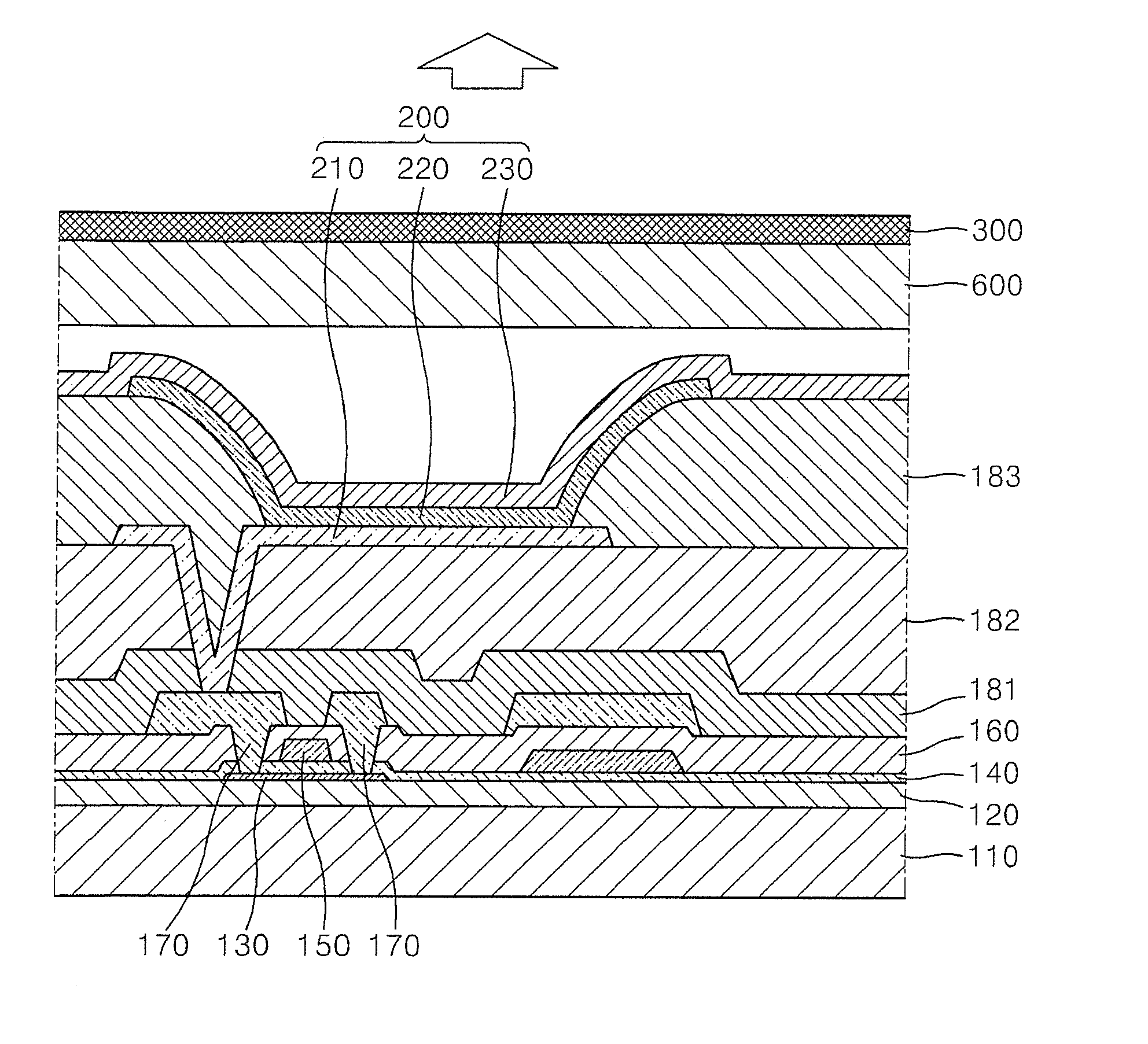
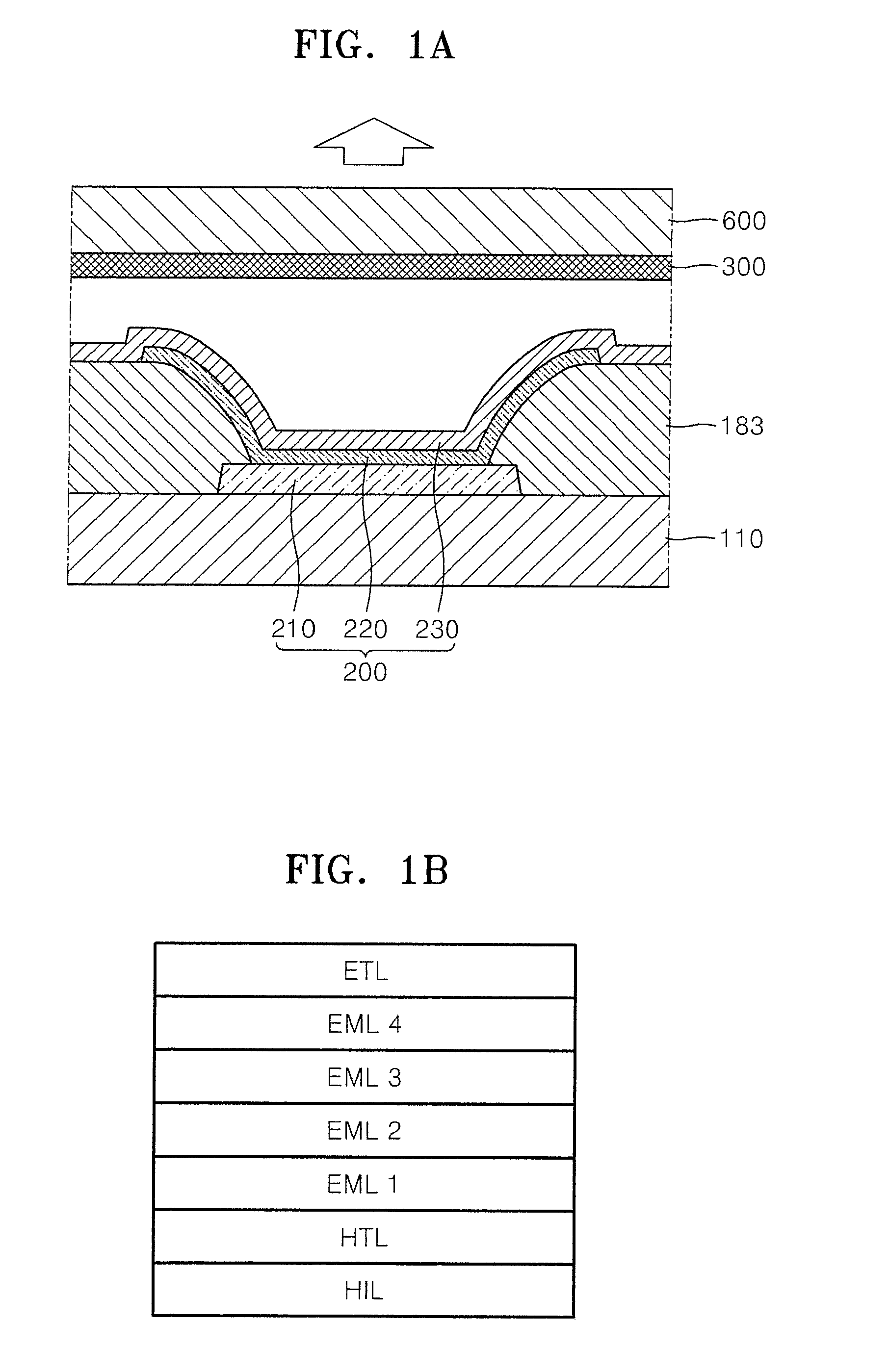
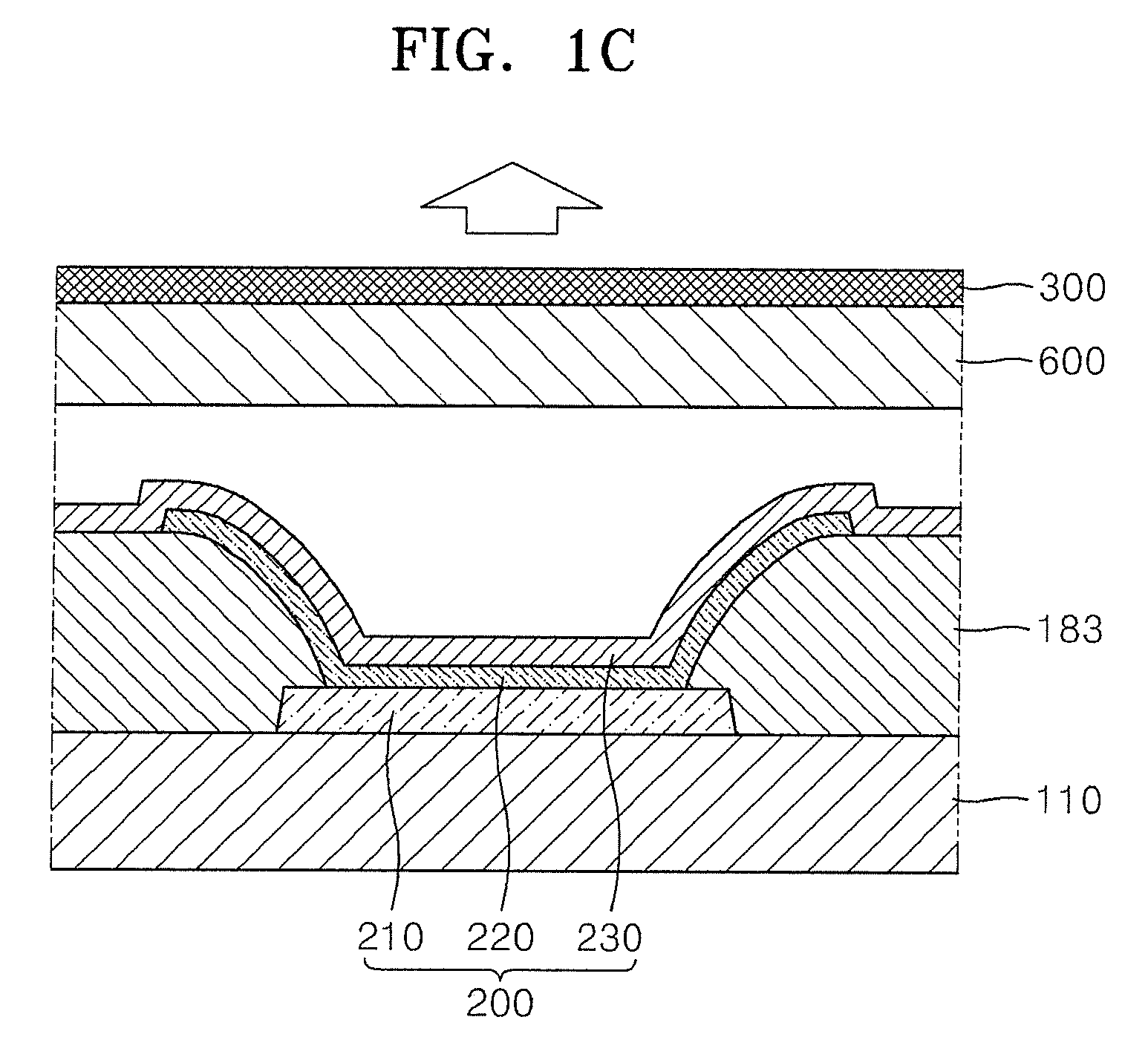
Organic light emitting device
- Summary
- Abstract
- Description
- Claims
- Application Information
AI Technical Summary
Benefits of technology
Problems solved by technology
Method used
Image

Examples
example 1
[0072]A Corning 15 Ω / cm2 (1200 Å) ITO glass substrate was cut into pieces of 50 mm×50 mm×0.7 mm in size. Then, each of the pieces was cleaned by sonification in isopropyl alcohol and deionized water for 5 minutes, and then the pieces were exposed to ultraviolet rays and UV ozone cleaned for 10 minutes. The pieces of glass substrate were installed in a vacuum deposition device.
[0073]NPD was vacuum deposited on the substrate to form a HIL. TPD was deposited on the HIL to form a HTL. 4,4-N,N-dicarbazole-biphenyl, constituting a host, and diphenyl-4-2-(1,1-; 4,1-terphenyl-4-yl-vinyl-phenyl) amine, constituting a deep blue dopant, were deposited on the HTL to form a first blue light emitting layer having a thickness of 8 nm.
[0074]4,4-N,N-dicarbazole-biphenyl (CBP), constituting a host, and fac-tris-(2-phenylpyridinato-N,C2) iridium-III (Ir(ppy)3, constituting a dopant, were deposited on the first blue light emitting layer to form a green light emitting layer having a thickness of 7 nm.
[0...
PUM
 Abstract
Description
Claims
Application Information