Thin film transistor array substrate and method of fabricating the same

a technology of thin film transistors and array substrates, which is applied in the direction of transistors, semiconductor devices, electrical devices, etc., can solve the problems of increasing the entire processing time and manufacturing cost, reducing the driving margin, and the thickness of the substrate may become non-uniform, so as to achieve a large contact area and increase the driving margin

Active Publication Date: 2010-07-01
SAMSUNG DISPLAY CO LTD
View PDF1 Cites 47 Cited by
  • Summary
  • Abstract
  • Description
  • Claims
  • Application Information

AI Technical Summary

Benefits of technology

[0008]This invention provides a TFT array substrate that increases a driving margin and provides a sufficiently large contact area between conductive materials in a contact portion.

Problems solved by technology

However, a photolithography process may include multiple steps, such as photoresist coating, mask arrangement, exposure, baking, development, and cleaning, thus increasing the entire processing time and the manufacturing cost.
However, if the passivation film is over-etched to form such an undercut, an insulating film on a storage electrode may be over-etched and its thickness may become non-uniform, thus causing a reduction in a driving margin.
Moreover, a data interconnection line may be damaged by over-etching, and etching of the data interconnection line in a contact area may cause a contact failure.

Method used


Image

  • Thin film transistor array substrate and method of fabricating the same
  • Thin film transistor array substrate and method of fabricating the same
  • Thin film transistor array substrate and method of fabricating the same

Examples


Embodiment Construction

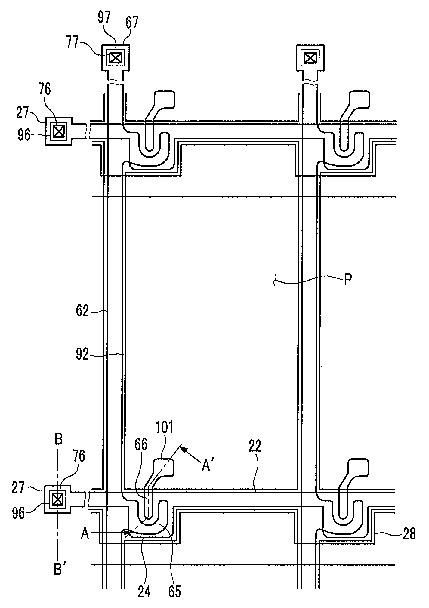
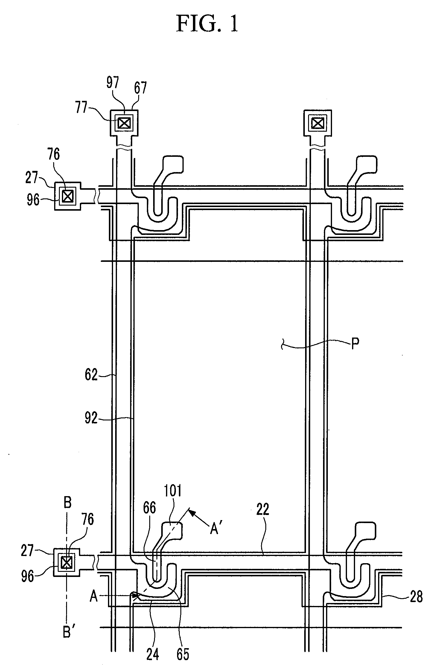
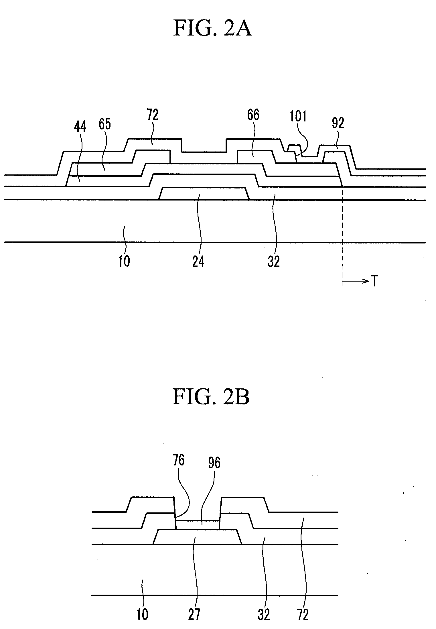
[0026]Advantages and features of the present invention and methods of accomplishing the same may be understood more readily by reference to the following detailed description of preferred embodiments and the accompanying drawings. The present invention may, however, be embodied in many different forms and should not be construed as being limited to the embodiments set forth herein. Rather, these embodiments are provided so that this disclosure will be thorough and complete and will fully convey the concept of the invention to those skilled in the art, and the present invention will only be defined by the appended claims. In the drawings, the thickness of layers and regions are exaggerated or reduced for clarity.

[0027]In the following description, it will be understood that when an element or a layer is referred to as being “on” or “connected to” another element or layer, it can be directly on or directly connected to the other element or layer, or intervening layers or elements may ...


PUM


Abstract

A method of fabricating a thin film transistor array substrate is presented. The method entails forming a gate interconnection line on an insulating substrate, forming a gate insulating layer on the gate interconnection line, forming a semiconductor layer and a data interconnection line on the semiconductor layer, sequentially forming multiple passivation layers, etching the passivation layers down to a drain electrode that is an extension of the data interconnection line. The portion of the drain electrode that is exposed at this stage is a part of the drain electrode-pixel electrode contact portion. A pixel electrode is formed connected to the drain electrode. Two of the passivation layers have the same composition but are processed at different temperatures. A thin film transistor prepared in the above manner is also presented.

Description

CROSS REFERENCE TO RELATED APPLICATION[0001]This application claims priority from and the benefit of Korean Patent Application No. 10-2008-0136895, filed on Dec. 30, 2008, which is hereby incorporated by reference for all purposes as if fully set forth herein.BACKGROUND OF THE INVENTION[0002]1. Field of the Invention[0003]The present invention relates to a thin film transistor (“TFT”) array substrate and a method of fabricating the same, and more particularly, to a TFT array substrate in which the manufacturing process may be simplified and manufacturing cost may be saved, and a method of fabricating the TFT array substrate.[0004]2. Discussion of the Background[0005]A liquid crystal display (“LCD”) includes two opposing display panels and a liquid crystal layer interposed therebetween. Each display panel may use a transparent insulating substrate as a supporting substrate. A plurality of thin film patterns may be formed on the insulating substrate. A thin film pattern formation incl...

Claims


Application Information

Patent Timeline
Patent Type & Authority Applications(United States)
IPC IPC(8): H01L29/786H01L29/24H01L21/336
CPCH01L27/1214H01L27/1225H01L27/1248H01L27/1288H01L29/7869
Inventor YANG, DONG-JUJEONG, YU-GWANGLEE, KI-YEUPKIM, SANG-GABYEO, YUN-JONGCHOI, SHIN-ILCHIN, HONG-KEECHOI, SEUNG-HABANG, JUNG-SUK
Owner SAMSUNG DISPLAY CO LTD
Why Eureka
Try Eureka