Bipolar Junction Transistor and Method of Manufacturing the Same

Inactive Publication Date: 2010-07-01
DONGBU HITEK CO LTD
View PDF2 Cites 6 Cited by
  • Summary
  • Abstract
  • Description
  • Claims
  • Application Information

AI Technical Summary

Benefits of technology

[0014]According to the present invention, a contact area of a junction region between the emitter and the base can be increased. As a result, a reverse saturation current and a current gain may increase and a

Problems solved by technology

However, when the depth of the base is decreased, the depletion layers of the emitter 130 and t

Method used


Image

  • Bipolar Junction Transistor and Method of Manufacturing the Same
  • Bipolar Junction Transistor and Method of Manufacturing the Same
  • Bipolar Junction Transistor and Method of Manufacturing the Same

Examples


Embodiment Construction

[0023]Reference will now be made in detail to specific embodiments of the present invention, examples of which are illustrated in the accompanying drawings. Wherever possible, the same reference numbers will be used throughout the drawings to refer to the same or like parts.

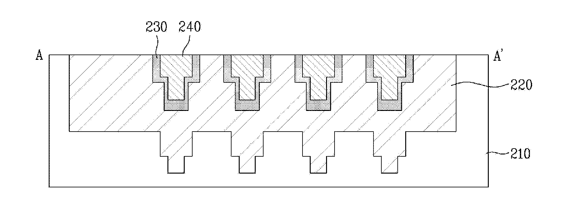
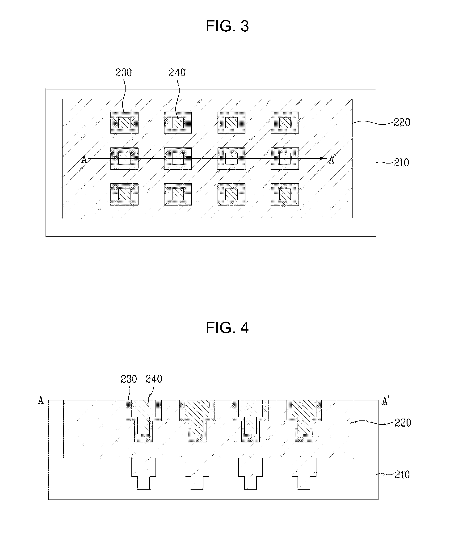
[0024]FIG. 3 is an overhead or layout view illustrating a bipolar junction transistor according to an exemplary embodiment of the present invention. FIG. 4 is a cross-sectional view of the bipolar junction transistor shown in FIG. 3 along the A-A′ line.

[0025]The bipolar junction transistor (BJT) includes a first conductivity type substrate 210 (e.g., a single-crystal silicon wafer, or a single-crystal silicon wafer with one or more layers of epitaxial silicon grown thereon), a base region 220 formed in the substrate 210, a plurality of step-shaped recesses formed in the base region 220 at an upper surface of the substrate, step-shaped polysilicon layers 240 deposited in each of the step-shaped recesses (the polys...


PUM


Abstract

A bipolar junction transistor and a method of manufacturing a bipolar junction transistor are disclosed. An exemplary bipolar junction transistor includes a second conductivity type base region in a first conductivity type substrate, step-shaped recesses in the base region, a polysilicon layer doped with a first conductivity type impurity in the step-shaped recesses, and a step-shaped emitter region between the polysilicon layer and the base region.

Description

CROSS REFERENCE TO RELATED APPLICATION[0001]This application claims the benefit of Korean Patent Application No. 10-2008-0138103, filed on Dec. 31, 2008, which is hereby incorporated by reference as if fully set forth herein.BACKGROUND OF THE DISCLOSURE[0002]1. Field of the Disclosure[0003]The present invention relates to a semiconductor device, more particularly, to a bipolar junction transistor (BJT) and a method of manufacturing the same.[0004]2. Discussion of the Related Art[0005]Generally, poly-emitter type bipolar junction transistors are suitable for high speed operation and they are operable in a high frequency range. Generally, a collector current increases in proportion to a reverse saturation current in a normal active mode of such a bipolar junction transistor (BJT).[0006]FIG. 1 is an overhead or layout view illustrating a conventional poly-emitter type bipolar transistor. FIG. 2 is a cross-sectional view of the bipolar junction transistor shown in FIG. 1 along the A-A′ ...

Claims


Application Information

Patent Timeline
IPC IPC(8): H01L29/73H01L21/331
CPCH01L29/1004H01L29/66303H01L29/73H01L29/7322H01L21/8248
Inventor LIM, HYON CHOL
Owner DONGBU HITEK CO LTD
Why Eureka
Try Eureka