Reflective TFT substrate and method for manufacturing reflective TFT substrate

a technology of reflective tft and substrate, applied in non-linear optics, instruments, optics, etc., can solve the problems of increased manufacturing cost, reduced production yield, complex production process, etc., and achieve the effect of improving connection reliability

Inactive Publication Date: 2010-07-01
INOUE KAZUYOSHI +3
View PDF8 Cites 77 Cited by
  • Summary
  • Abstract
  • Description
  • Claims
  • Application Information

AI Technical Summary

Benefits of technology

[0054]By doing this, for example, if a metal layer is used as the gate wire, the metal surface can be prevented from being exposed when an opening for a gate wire pad is formed, whereby connection reliability can be improved.

Problems solved by technology

So many production steps may decrease production yield.
In addition, many steps may make production process complicated and also increase manufacturing cost.

Method used


Image

  • Reflective TFT substrate and method for manufacturing reflective TFT substrate
  • Reflective TFT substrate and method for manufacturing reflective TFT substrate
  • Reflective TFT substrate and method for manufacturing reflective TFT substrate

Examples


Embodiment Construction

One Embodiment of the Method for Producing a Reflective TFT Substrate

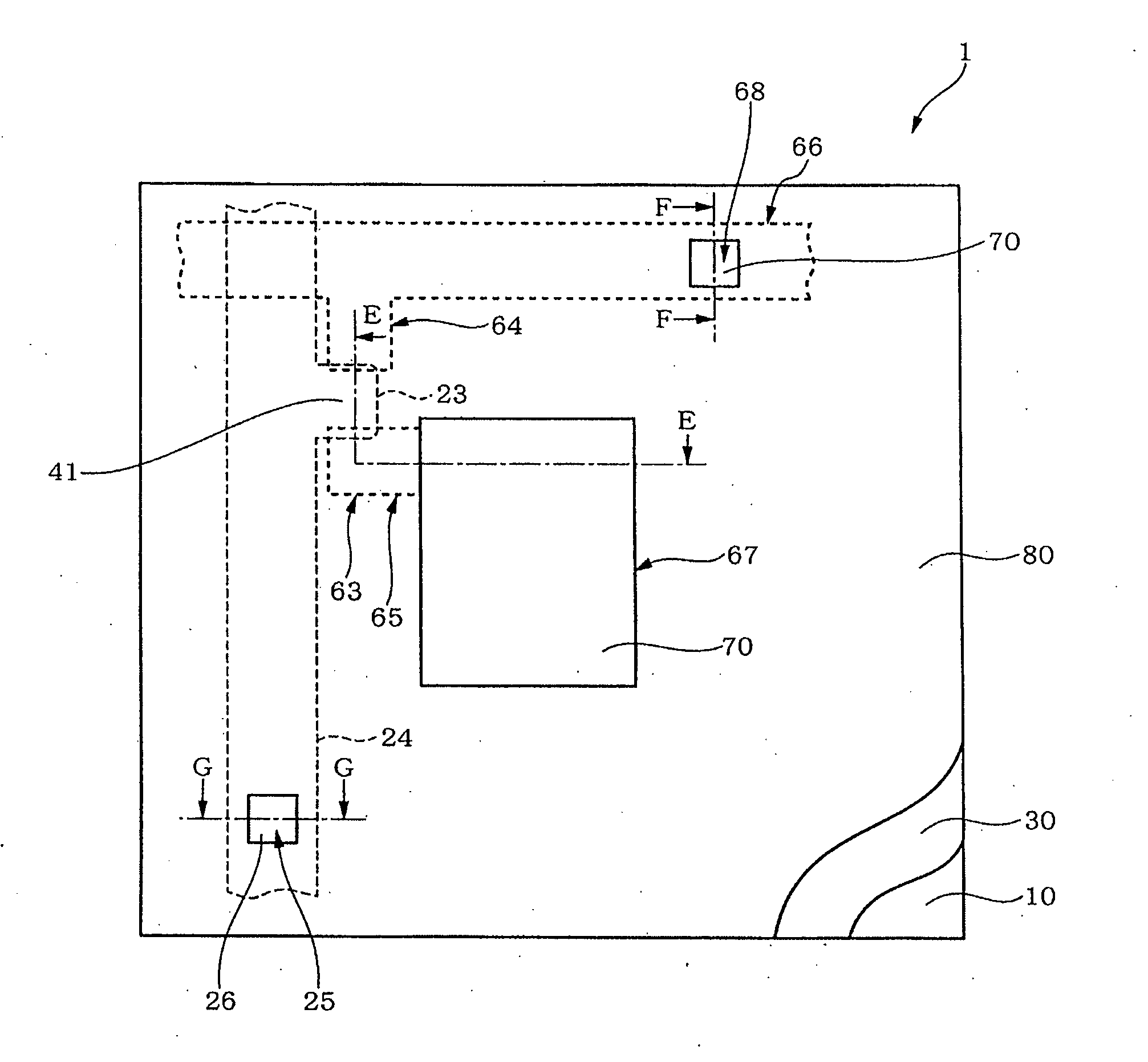
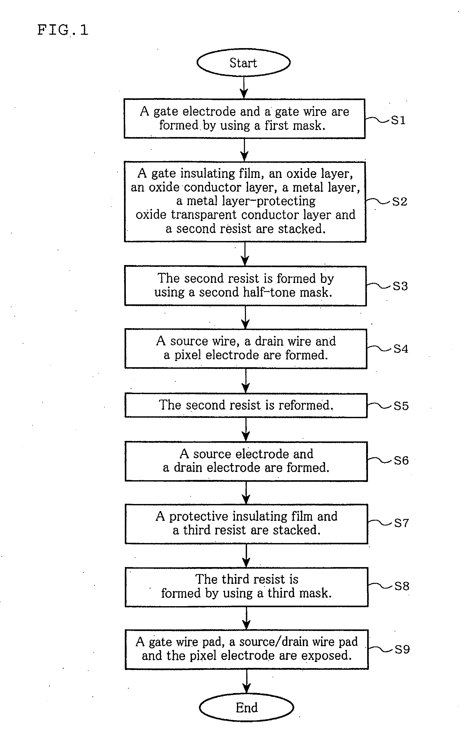
[0066]FIG. 1 is a schematic flow chart for explaining the method for producing a reflective TFT substrate according to one embodiment of the invention.

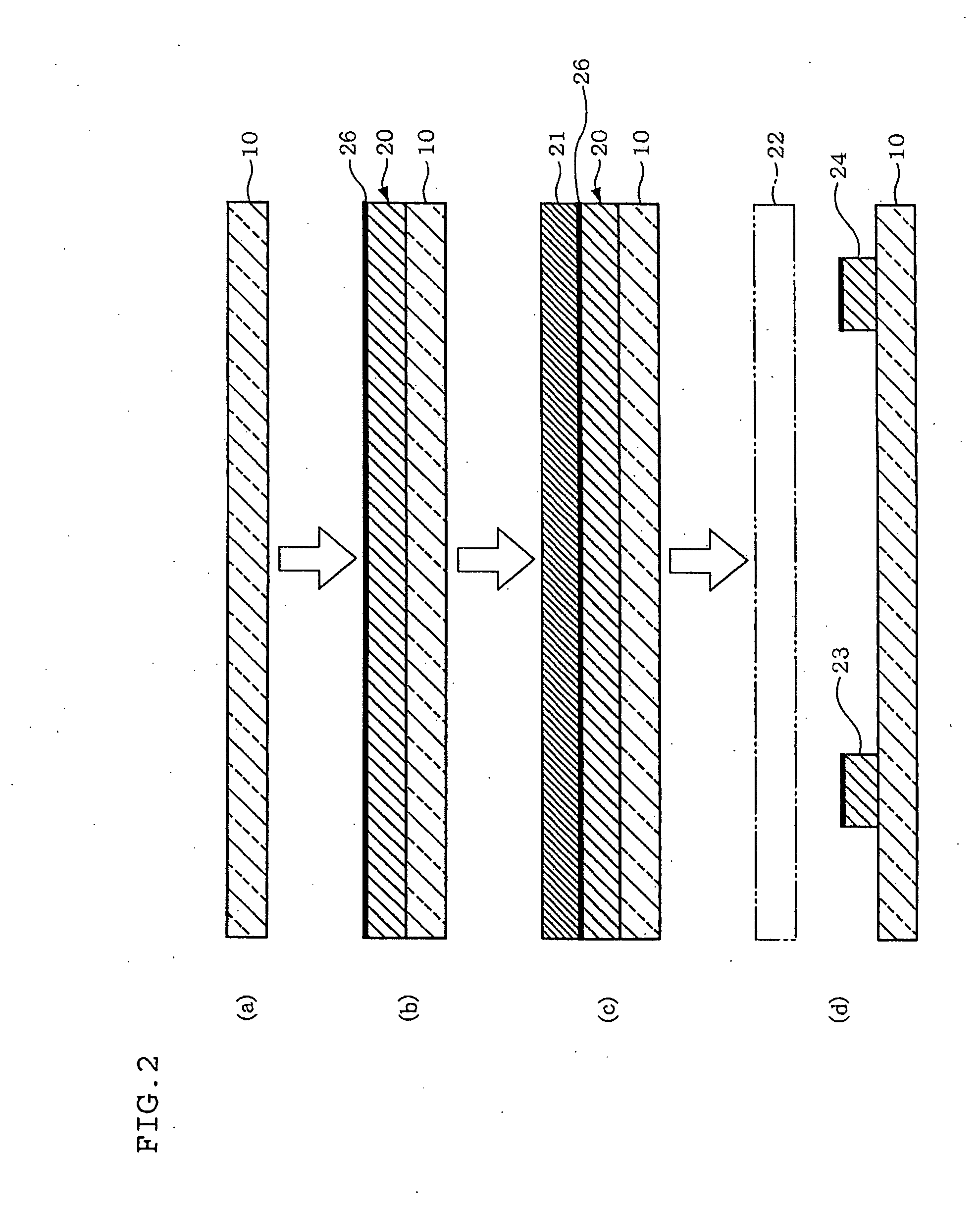
[0067]In FIG. 1, first, a gate electrode 21 and a gate wire 22 are formed on a substrate 10 by using a first mask 22 (Step S1). Then, treatment using the first mask 22 will be explained with reference to the drawing.

Treatment Using a First Mask

[0068]FIG. 2 is a schematic view for explaining treatment using a first mask in the method for producing a reflective TFT substrate according to one embodiment of the invention. (a) is a cross-sectional view of a glass substrate before treatment. (b) is a cross-sectional view after the formation of a metal, layer / the formation of a metal layer-protecting oxide transparent conductor layer. (c) is a cross-sectional view after the application of a first resist. (d) is a cross-sectional view after exposure / development / first etching...


PUM


Abstract

A reflective TFT substrate which can be operated for a prolonged period of time due to the presence of a protective insulating film, is free from occurrence of crosstalk, and is capable of significantly reducing manufacturing cost by decreasing the production steps in the production process. A reflective TFT substrate 1 comprises a substrate 10; a gate electrode 23 and a gate wire 24; a gate insulating film 30; an n-type oxide semiconductor layer 40; a metal layer 60 formed with a channel part 41 interposed therebetween; and a protective insulating film 80 which covers the upper part of the glass substrate 10 on which a pixel electrode 67, a drain wire pad 68 and a gate wire pad 25 are exposed, wherein the metal layer 60 functions at least as a source wire 65, a drain wire 66, a source electrode 63, a drain electrode 64 and the pixel electrode 67.

Description

TECHNICAL FIELD[0001]The invention relates to a reflective TFT substrate and a method for producing a reflective TFT substrate. In particular, the reflective TFT substrate of the invention comprises an oxide semiconductor layer, a metal layer and a protective insulating film. The oxide semiconductor layer is an active layer of a TFT (Thin Film Transistor). The metal layer is formed above the oxide semiconductor layer with a channel part interposed therebetween, and functions as a source wire, a drain wire, a source electrode, a drain electrode and a pixel electrode. Due to such a configuration, the reflective TFT substrate of the invention can be operated stably for a prolonged period of time. In addition, according to the invention, not only manufacturing cost can be decreased due to the reduction of production steps but also concern for occurrence of interference of gate wires (crosstalk) can be eliminated.BACKGROUND[0002]LCD (Liquid Crystal Display) apparatuses or organic EL disp...

Claims


Application Information

Patent Timeline
Patent Type & Authority Applications(United States)
IPC IPC(8): H01L27/088H01L21/28
CPCG02F1/133553G02F1/1368H01L27/1225H01L29/45H01L29/7869H01L27/1288G02F1/13439
Inventor INOUE, KAZUYOSHIYANO, KOKITANAKA, NOBUOTANAKA, TOKIE
Owner INOUE KAZUYOSHI
Why Eureka
Try Eureka