

Methods of forming nickel sulfide film on a semiconductor device
a technology of nickel sulfide film and semiconductor device, which is applied in the direction of semiconductor/solid-state device details, coatings, chemical vapor deposition coatings, etc., can solve the problems of non-conform metal deposition on three-dimensional (3d) features of 3d transistor structures and difficulty in depositing metal at the bottom of high aspect ratio features
- Summary
- Abstract
- Description
- Claims
- Application Information
AI Technical Summary
Problems solved by technology
Method used
Image

Examples
Embodiment Construction
[0015]In the following description, numerous specific details are set forth in order to provide a thorough understanding of the present invention. In other instances, well known semiconductor processing techniques and features have not been described in particular detail in order not to unnecessarily obscure the present invention.
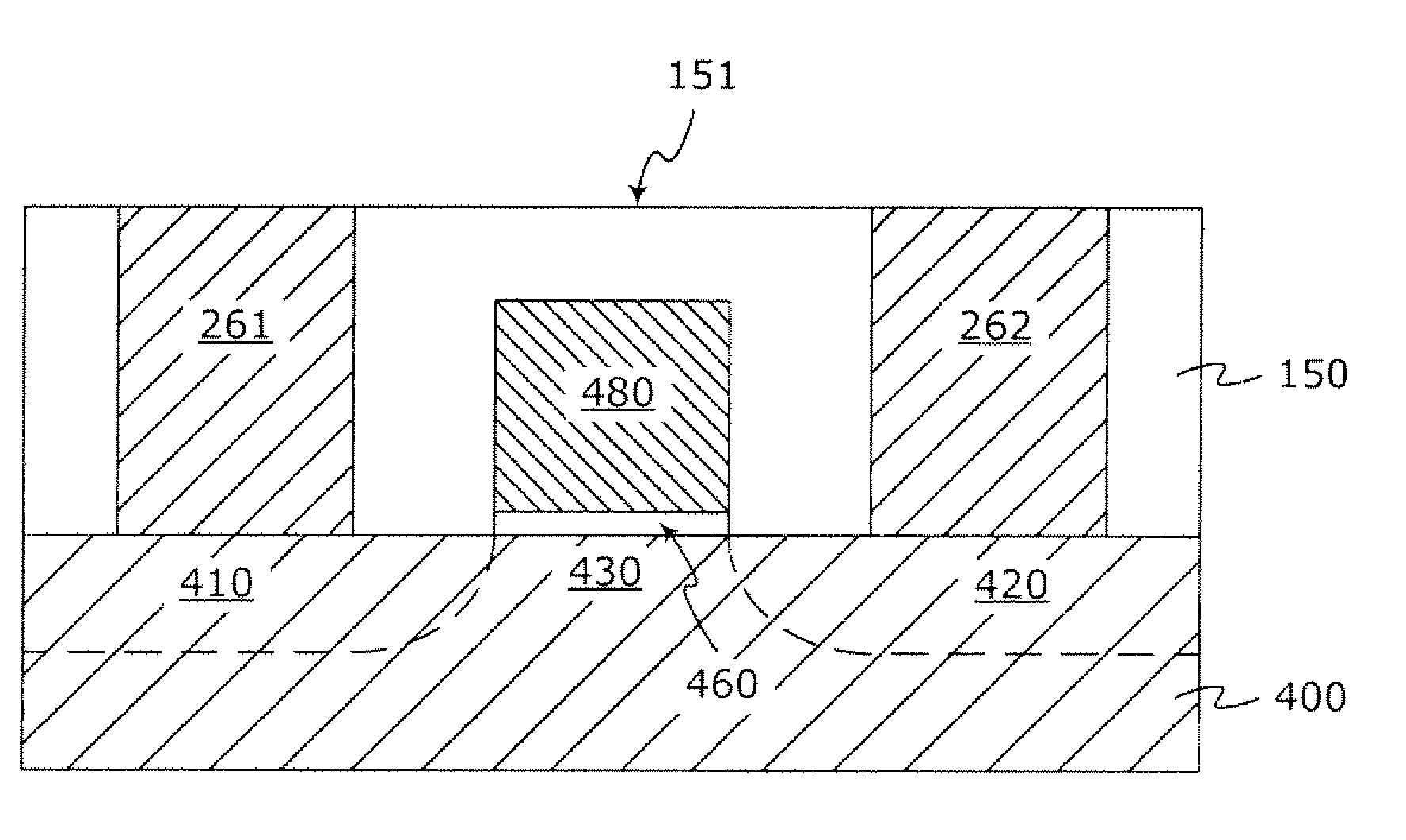
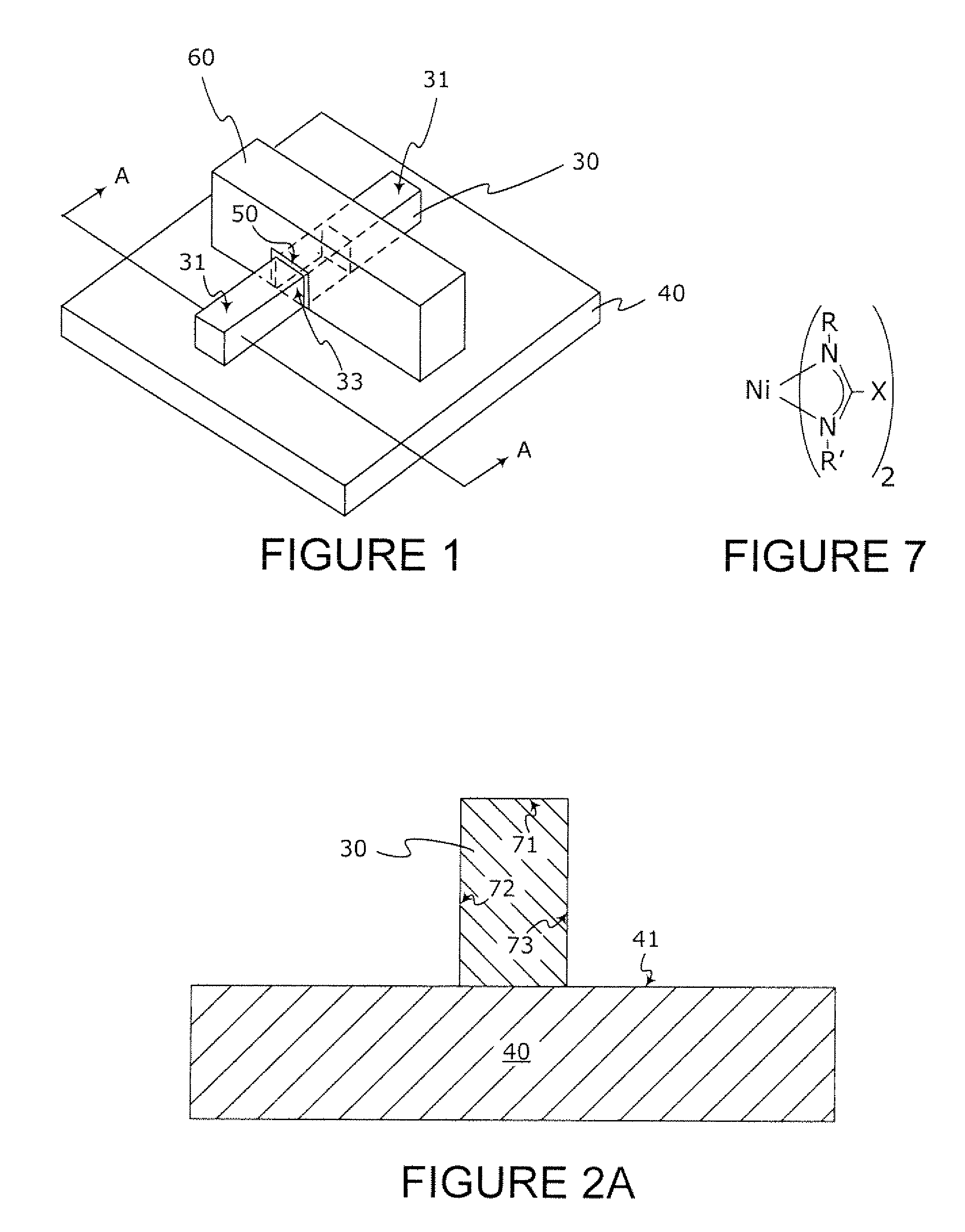
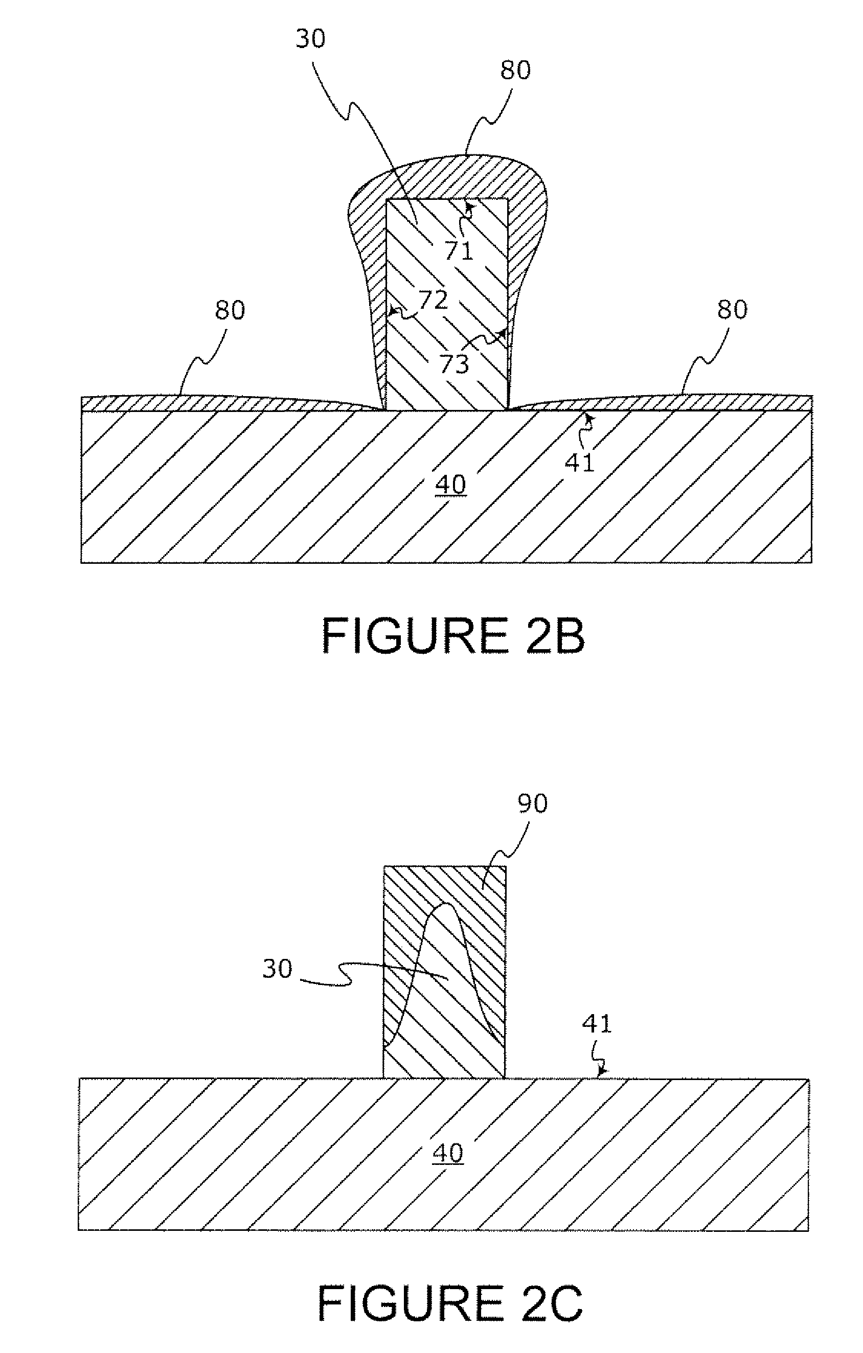
[0016]Embodiments of the present invention describe a method of forming nickel sulfide layer on a semiconductor device. In an embodiment of the present invention, the semiconductor device comprises a substrate or a semiconductor body. A nickel sulfide layer is conformally deposited on the substrate or semiconductor body by alternatingly exposing the substrate or semiconductor body to a nickel-containing precursor and a sulfur-containing precursor. For example, the nickel containing precursor can be a nickel organometallic compound and the sulfur-containing precursor can be hydrogen sulfide. The nickel sulfide layer can be used for contact applications, cont...
PUM
| Property | Measurement | Unit |
|---|---|---|
| constant temperature | aaaaa | aaaaa |
| pressure | aaaaa | aaaaa |
| constant temperature | aaaaa | aaaaa |
Abstract
Description
Claims
Application Information