

Apparatus for pulling silicon single crystal
a silicon single crystal and apparatus technology, applied in the direction of crystal growth process, polycrystalline material growth, under a protective fluid, etc., can solve the problem of reducing oxygen concentration, and achieve the effect of suppressing the heterogeneous distribution of impurity concentration, reducing magnetic field strength, and inhibiting the fluctuation of resistivity
- Summary
- Abstract
- Description
- Claims
- Application Information
AI Technical Summary
Benefits of technology
Problems solved by technology
Method used
Image

Examples
examples
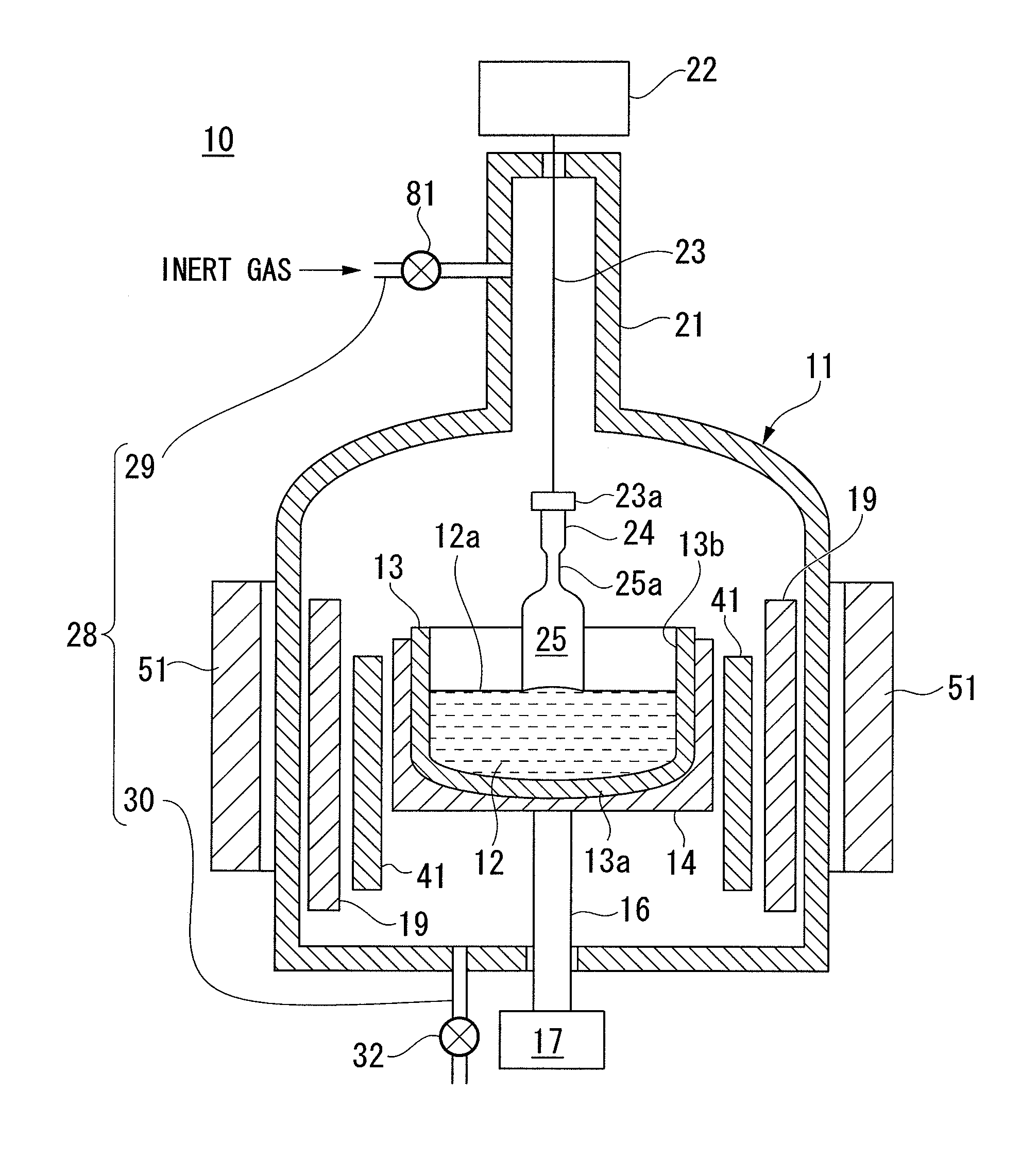
[0067]The inventors examined the action and effect of the invention. In the examination process, firstly, a quartz crucible having a diameter of 24 inches was prepared. Polycrystalline silicon of 160 kg was charged in the crucible as a raw material. Then, the quartz crucible charged with the raw material was heated by a heater thereby forming a silicon melt. A silicon single crystal ingot having a diameter of 200 mm was pulled from the melt. In the pulling process, a horizontal magnetic field was applied to the silicon melt in the quartz crucible using a space-saving type horizontal field magnet (magnetic field applying unit). In the horizontal field magnet, magnetic coils were deformed and installed in a ring-shaped case which was arranged to surround the chamber of the silicon single crystal pulling apparatus.
[0068]The application of the horizontal magnetic field to the silicon melt was performed in accordance with three examples according to the present invention.
[0069]In the fir...
PUM
| Property | Measurement | Unit |
|---|---|---|
| diameter | aaaaa | aaaaa |
| diameter | aaaaa | aaaaa |
| diameter | aaaaa | aaaaa |
Abstract
Description
Claims
Application Information