Display and method for manufacturing display

a technology of display and display element, applied in the field of display, can solve the problems of increasing the thickness of the film, the off current of the transistor, and the difficulty of obtaining a sufficient sensor sensitivity, so as to enhance the sensitivity enhance the effect of the light sensor elemen

Active Publication Date: 2010-07-08
JAPAN DISPLAY WEST
View PDF5 Cites 37 Cited by
  • Summary
  • Abstract
  • Description
  • Claims
  • Application Information

AI Technical Summary

Benefits of technology

[0013]In the display and the method for manufacturing the same according to the present invention, by a configuration in which the light absorption coefficient of a second active layer for constituting light sensor elements is set to be higher than that of a first active layer for constituting switching elements, the sensitivity characteristic of the light sensor elements can be controlled separately from the switching elements. Therefore, the sensitivity of the light sensor elements can be enhanced, without changing the characteristics of the switching elements.
[0014]Besides, in the method for manufacturing the display according to the present invention, by a configuration in which a second active layer is formed over the same underlying layer as that for active layer of 1 for constituting switching elements, in a layer thickness different from that of the first active layer or by use of a material different from the material for the first active layer, the sensitivity characteristic of the light sensor elements can be controlled separately from the switching elements. Therefore, the sensitivity of the light sensor elements can be enhanced, without changing the characteristics of the switching elements.
[0015]According to the present invention, the sensitivity of light sensor elements can be enhanced without influencing the characteristics of switching elements, in a display equipped with light sensors.

Problems solved by technology

In the displays equipped with light sensors according to the related art, therefore, most of the light externally incident on the light sensor element would be transmitted through the photoelectric conversion layer, making it very difficult to obtain a sufficient sensor sensitivity.
In the case of the poly-Si TFT, however, an increase in the film thickness leads to problems such as a rise in the OFF current of transistor, an increase in light leakage, and a difficulty in crystallization by a laser annealing treatment using an excimer laser.
In the case of the a-Si:H TFT, also, an increase in the film thickness leads to problems such as a rise in the OFF current, an increase in S-D resistance, and an increase in light leakage.

Method used


Image

  • Display and method for manufacturing display
  • Display and method for manufacturing display
  • Display and method for manufacturing display

Examples


first embodiment

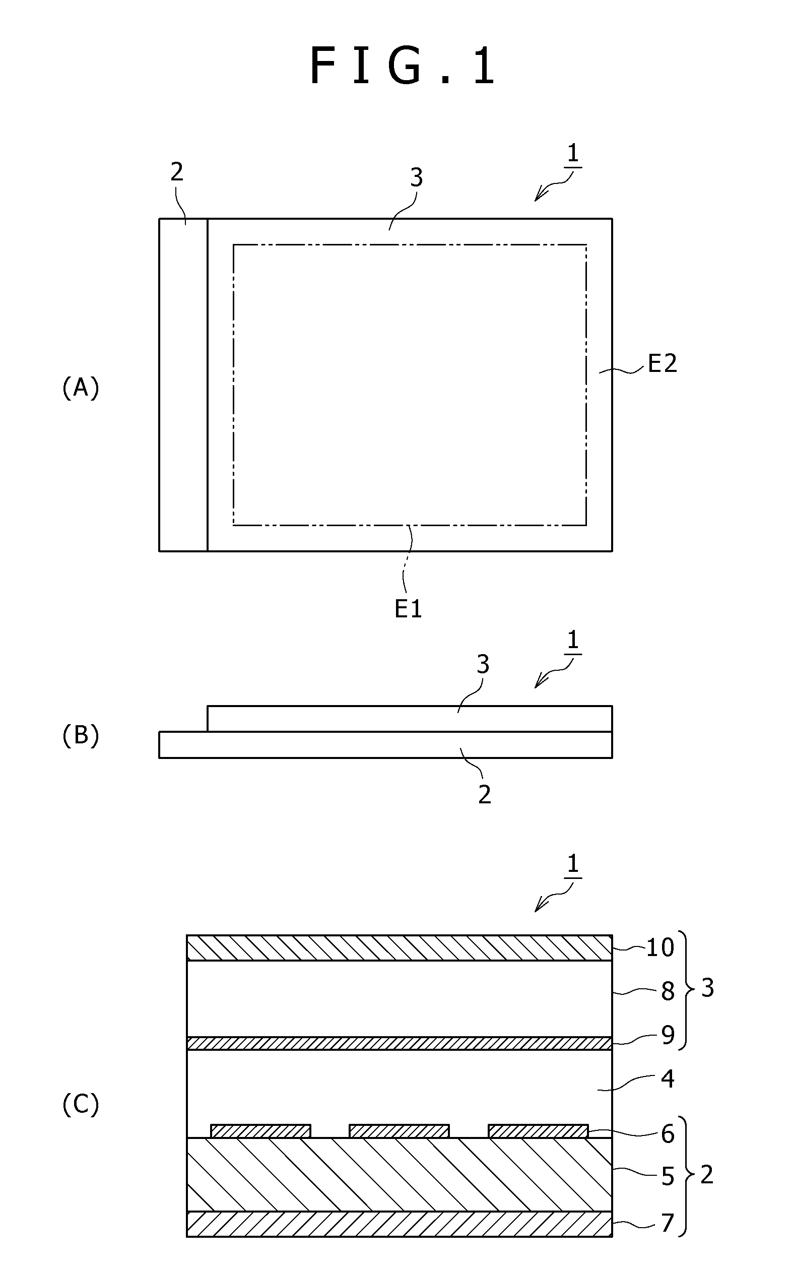
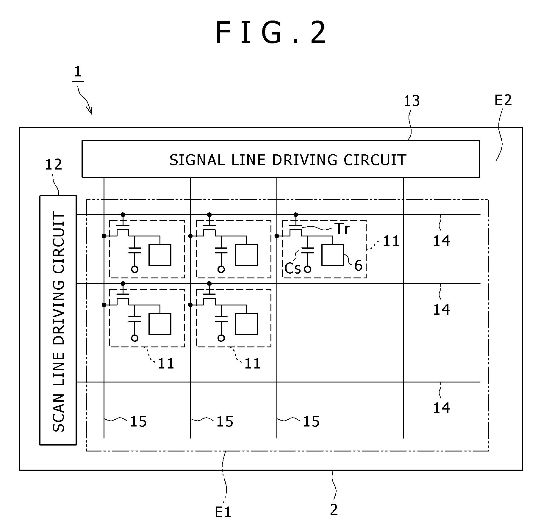
[0061]FIG. 5 is a sectional view showing a main part of a driving substrate 2 of a liquid crystal display 1 according to a first embodiment of the present invention. As shown in the figure, over a glass substrate 5 serving as a base of the driving substrate 2, first element forming portions 21 for configuring switching elements (thin film transistors Tr) for pixels 11 and second element forming portions 22 for configuring light sensor elements 101 of sensor parts 100 are provided. In plan view of the glass substrate 5 as viewed from the side of the liquid crystal layer 4 shown in FIG. 1, the first element forming portions 21 are arranged in the display area E1 together with the pixels 11, and the second element forming portions 22 are arranged in the display area E1 together with the sensor parts 100. It is to be noted here, however, that this configuration is not limitative; for example, the first element forming portions 21 may be arranged in both the display area E1 and the perip...

second embodiment

[0081]FIG. 8 is a sectional view showing a main part of a driving substrate 2 in a liquid crystal display 1 according to a second embodiment of the present invention. The second embodiment differs from the above-described first embodiment, particularly in that a light reflecting film 40 is provided on a gate electrode 33 in a second element forming portion 22. The light reflecting film 40 is formed on a surface of the gate electrode 33 which is disposed closest to and opposite to the photoelectric conversion layer 35 on the side opposite to the side of incidence of external light. In addition, the light reflecting film 40 is formed by use of a metallic material which is at least higher than the gate electrode 33 in reflectance, for example, silver.

[0082]With the light reflecting film 40 thus provided so as to cover the gate electrode 33, the light having externally entered and passed through the photoelectric conversion layer 35 is efficiently reflected by the light reflecting film ...

third embodiment

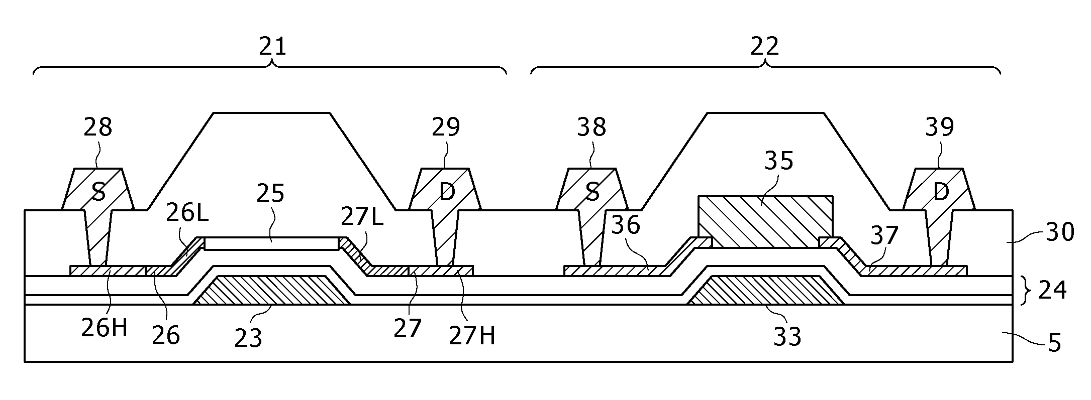
[0093]FIG. 12 is a sectional view showing a main part of a driving substrate 2 in a liquid crystal display 1 according to a third embodiment of the present invention. The third embodiment differs from the above-described first embodiment, particularly in that a transparent electrode is used as a gate electrode 23 in a first element forming portion 21 for realizing a transparent LCD (Liquid Crystal Display), that sources 26, 36 and drains 27, 37 are each formed by a transparent conductive film, that transparent electrodes are used as source electrodes 28, 38 and drain electrodes 29, 39, that a channel layer 25 is formed by a transparent semiconductor film, that a gate electrode 33 is formed as a metallic shielding electrode, and that second element forming portions 22 are arranged only in a peripheral area E2.

[0094]The gate electrode 23 is formed by use of a transparent conductive material, for example, ITO. The sources 26, 36 and the drains 27, 37 are each formed by use of a transpa...


PUM


Abstract

In the case of forming switching elements and light sensor elements over the same substrate, an increase in the film thickness of active layers in an attempt to enhance the sensitivity of the light sensor elements would adversely affect the characteristics of the switching elements (TFTs). In a configuration of a display in which a channel layer 25 for constituting thin film transistors to form the switching elements for pixels and a photoelectric conversion layer 35 for constituting the light sensor elements are provided over a gate insulating film 24 on a glass substrate 5 to be provided with a plurality of pixels arranged in a matrix pattern, the photoelectric conversion layer 35 is formed to be thicker than the channel layer 25, and / or the photoelectric conversion layer 35 is formed of a material different from the material for the channel layer 25, whereby the light absorption coefficient of the photoelectric conversion layer 35 is made to be higher than that of the channel layer 25.

Description

TECHNICAL FIELD[0001]The present invention relates to a display integrally provided with light sensors and a method for manufacturing the same.BACKGROUND ART[0002]Recently, liquid crystal displays using a-Si:H (hydrogenated amorphous silicon) TFTs or poly-Si (polycrystalline silicon) TFTs are provided with an automatic back-light adjusting function or a touch screen function utilizing light sensors. In this type of liquid crystal displays, light sensor elements are configured with the same structure as that of thin film transistors (TFTs) provided as switching elements for pixels (refer to, for example, Japanese Patent Laid-open No. 2007-018458). Therefore, it is possible to inexpensively provide a display equipped with light sensors, without spoiling such advantageous features as reduced size and reduced thickness.[0003]Hitherto, a layer contributing to photoelectric conversion by sensing light in the light sensor element (the layer will hereinafter be referred to as “photoelectric...

Claims


Application Information

Patent Timeline
Patent Type & Authority Applications(United States)
IPC IPC(8): H01L33/08H01L21/28
CPCG02F1/1368G02F2001/13312G06F3/0412H01L27/1222H01L27/1214H01L29/66765H01L27/124G06F3/0421G02F1/13312G09F9/30H01L31/10
Inventor GOSAIN, DHARAM PALTANAKA, TSUTOMUTAKATOKU, MAKOTO
Owner JAPAN DISPLAY WEST
Why Eureka
Try Eureka